
Methods for Thin Film Thickness Measurement
Thin films are deposited layers or coatings with thicknesses in the range of micrometer or nanometer that are widely used in various industries including electronics, nanotechnology, energy, and industrial coatings. One of the main challenges in working with these films is the accurate measurement of their thickness, which is central in PVD process control, metrology and materials research.


How to choose the proper method for measurement of thin film thickness?
Thin film thickness measurement can be performed in various ways and can monitor the thickness in-situ (real-time feedback during deposition) and ex-situ characterization (post-deposition measurements often used for absolute calibration and high-accuracy metrology), each with its own advantages and disadvantages. The proper choice of thickness measurement method depends on the optical/electrical properties of the film and its thickness range, required accuracy, process constraints (vacuum vs. ambient), and whether the measurement should be non-destructive. In this article, we will review the different methods for measuring film thickness.
1. Optical Methods
One of the simplest and most widely used methods for measuring the thickness of thin films is the use of optical instruments. This method takes advantage of the property of light reflection from a surface. The reflection of light beams may result in changing the polarization of beams electric field and formation of interference patterns, from which the film thickness can be calculated.
1.1. White Light Reflectometry
If the reflected lights from the film and the underlying substrate interfere properly, interference patterns will be visible. Knowing the refractive index of the thin film, the thickness of the layer can be determined by in-situ monitoring of the changes in these patterns. White light reflectometry is a non-destructive thickness measurement method with sub-nanometer accuracy that is commonly used in industrial PVD systems.
1.2. Interferometry
Interferometry is one of the most accurate methods for measuring the thickness of thin layers. In this method, laser light beams hit the surface of the sample covered by a thin film, where part of them are refracted from the surface of the layer and part from the substrate, ultimately leading to the formation of interference patterns. By analyzing these patterns, the thickness of the layer can be calculated with high accuracy. This method is very popular due to its high accuracy in measuring small thicknesses (Up to a few nanometers).
1.2.1. Fresnel Diffraction
Fresnel diffraction fringes are created on a screen perpendicular to the reflected beam when a parallel coherent beam of monochromatic light illuminates a thin film that has been manufactured in a step form on a substrate and uniformly coated with a reflecting material. The film thickness, angle of incidence, and wavelength of light all affect how visible the fringes are. The film thickness can be determined with an accuracy of a few nanometers by measuring visibility versus incident angle. The method is simple to use and yields highly reliable results across a broad range of thicknesses.


1.3. Reflectance Spectroscopy
This method is based on measuring changes in the reflection of light beams with different wavelengths from the surface of thin layers. When light hits the thin layer, part of it is reflected, where the amount of reflection alters with the thickness of the layer and the light wavelengths, leading to measurement of thin film thickness. This method is particularly useful for thin metal layers and insulators.
1.4. Ellipsometry
Ellipsometry measures the change in the polarization of a spectrum of light beam after reflection from the thin film surface, which yields film thickness (in the range of sub-nanometer to several microns) and optical constants. This method can be performed to monitor in-situ film deposition process, as well as after deposition (ex-situ) to extract thickness and optical constants.
A quarter wave plate polarizes the incident beam before reflection from the thin film. The polarizer and analyzer are rotated so as to obtain the null on the photomultiplier.
2. AFM and Profilometry
In mechanical methods, an instrument is used to make a direct contact with the layer surface and measure the thickness of thin layers.
2.1. Atomic force microscopy (AFM)
Atomic force microscopy, introduced in 1986, is one of the methods for examining the surface structure and measuring the thickness of thin layers, providing high-resolution topography and measuring ultrathin films and step heights with sub-nanometer vertical resolution. This method uses a very sharp needle that is brought close to the layer surface and by measuring the force applied to the needle, precise information about the layer thickness and surface properties can be obtained over small areas (µm scale).
2.2. Profilometry
Stylus (contact) profilometry measures step heights of the films, which can be patterned or scratched to expose substrate and scan with a stylus to read step height directly. It is direct and instrumentally simple, and accurate for steps from a few nanometers up to tens of micrometers, with a typical resolution of a few nanometers.
3. X-Ray Methods
Using X-rays to measure the thickness of thin films is one of the advanced and accurate methods. In this method, X-rays are irradiated to the surface of the film and the amount of absorption or scattering of the radiation by the film is examined.
3.1. X-Ray Reflectivity (XRR)
Thickness measurement of thin films by X-ray reflectivity is a high-accuracy, non-destructive technique for various coatings (typically 0.5–200 nm), extendable with the right setup). XRR fits Kiessig fringes in grazing-incidence reflectivity to extract layer thickness, density and interface roughness with Å–nm precision for smooth layers. It is especially valued for precise metrology in thin, smooth films and multilayers.
3.2. X-Ray Diffraction
X-ray diffraction (XRD) is particularly used for thin crystalline films. In this method, X-rays reach the surface of the film, reflect from the film surface and the beneath substrate, resulting in formation of scattering patterns. From these patterns, information about the crystal structure and thickness of the film can be obtained.
3.3. Effects of X-Ray Fluorescence
This method can be used indirectly to measure the thickness of thin films. In this method, X-ray irradiation of the film surface produces fluorescence radiation from the elements present in the film. The amount of this radiation can be related to the film thickness.
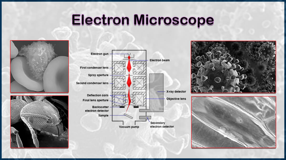
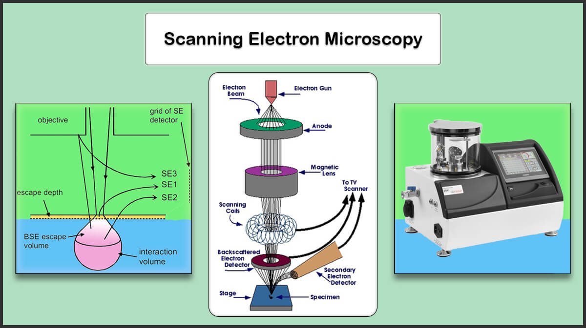
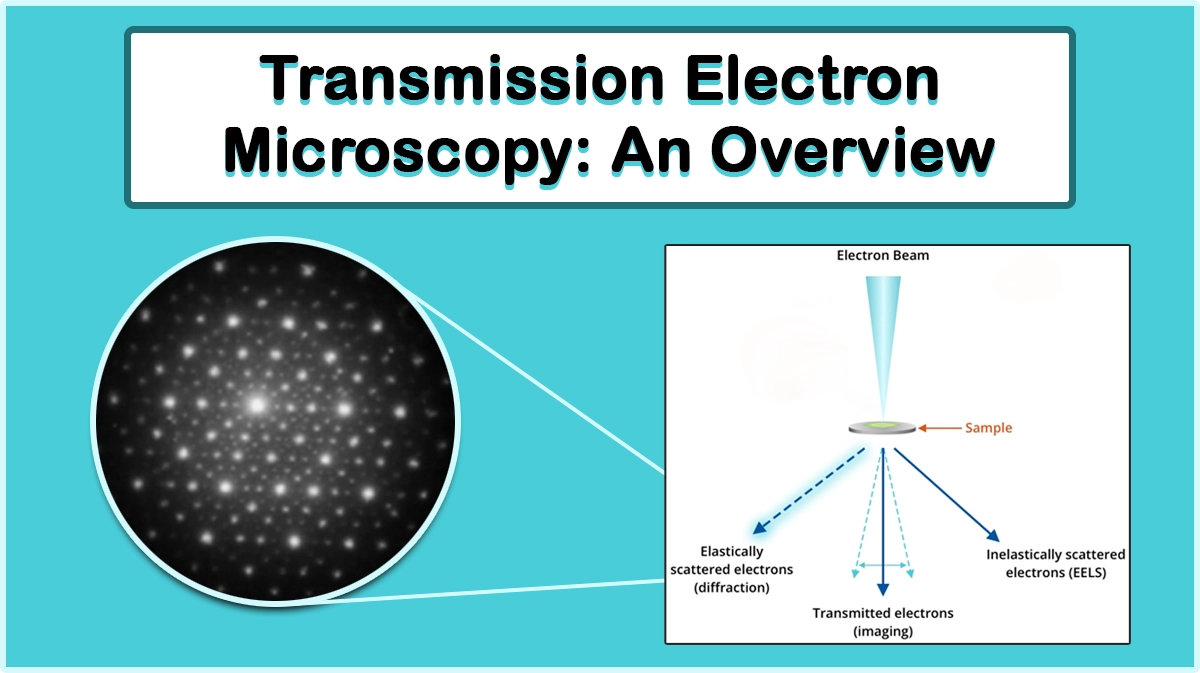
4. SEM and TEM Cross Sectional Thickness Measurement
Electron microscopy (SEM/TEM) cross-sectioning can give structural information and thickness measurement of thin films. SEM cross-sections, which is typically prepared by focused ion beam) can measure film thickness of a few nm and more, with spatial resolution down to a few nm, while TEM offers atomic-scale resolution for very thin films but requires intricate sample preparation step. These techniques require sample cross-sectioning, so are destructive, but yield clear data on thin films thickness and microstructure.
5. Other Methods
When a surface is covered by a thin film, its properties may alter relating to the thin film thickness, such as thermoelectric properties, electrical resistivity, or acoustic resonating waves, which can be used to measure the layer thickness.
4.1. Resonator-Based Mass Sensors (QCM)
The quartz crystal microbalance (QCM) is a technique for in-situ monitoring of deposition thickness and rate in physical vapor deposition process. A QCM crystal senses the mass increase on the resonating quartz crystal and the sensor reports thickness via the Sauerbrey relation, according to the film density. QCM is fast, compact and readily integrated into deposition chambers; it is most accurate for thin, rigid films where viscoelastic effects are small. Typical resolution is sub-monolayer mass (frequency resolution of ~1 Hz on a 5 MHz crystal), translating to thickness sensitivity of fractions of a nanometer depending on density.


Application Notes
Methods such as interferometry and atomic force microscopy are ideal for very thin films due to their high accuracy and the ability to measure nanometer thicknesses. However, methods such as electrical resistivity analysis and four-point bridge are more suitable for thicker films.
In X-ray diffraction (XRD) and X-ray fluorescence (XRF), the accuracy is highly dependent on the type and properties of the film material and its structure. These methods are particularly accurate for crystalline or metallic films.
In the following, various parameters of different methods for thin film thickness measurement are compared in a table.
Conclusion
Thickness measurement of thin films is a crucial step in industrial and research processes. The choice of the appropriate method depends on the type of material, the required accuracy, and the process constraints. In-situ and ex-situ optical methods are very popular due to their high accuracy and non-destructiveness, while QCM sensors provide fast feedback for rate control. The XRR, profilometry and cross-section TEM/SEM are typically used for calibration and to validate models.
References
- Vedam, K. (1998). Spectroscopic ellipsometry: a historical overview. Thin solid films, 313, 1-9.
- Van Duren, S., Levcenco, S., Kretzschmar, S., Just, J., & Unold, T. (2019). Investigation of reflectometry for in situ process monitoring and characterization of co-evaporated and stacked Cu-Zn-Sn-S based thin films. Journal of Alloys and Compounds, 779, 870-878.
- Ogieglo, Wojciech, et al. “Spectroscopic ellipsometry analysis of a thin film composite membrane consisting of polysulfone on a porous α-alumina support.” ACS applied materials & interfaces 4.2 (2012): 935-943.
- Review of x-ray and optical thin film measurement methods and transfer artefacts,
- Acosta, G., Allred, D. D., & Davis, R. C. (2005). A Technique for Measuring the Thin Film Thickness of Ultrathin Metallic Thin Films, 4-20 nm, using Atomic Force Microscopy. Nqhfhmk Bnmsqhatsdc@ qshbkdr9.
-
Hues, S. M., Colton, R. J., Meyer, E., & Güntherodt, H. J. (1993). Scanning probe microscopy of thin films. MRS Bulletin, 18(1), 41-49.
- Maniscalco, B., Kaminski, P. M., & Walls, J. M. (2014). Thin film thickness measurements using scanning white light interferometry. Thin Solid Films, 550, 10-16.
- http://sites.science.oregonstate.edu
-
Eckertová, L. (1977). Thin Film Thickness and Deposition Rate Measurement Methods. In: Physics of Thin Films. Springer, Boston, MA. https://doi.org/10.1007/978-1-4615-7589-4_3
- Piegari, A., & Masetti, E. (1985). Thin film thickness measurement: a comparison of various techniques. Thin solid films, 124(3-4), 249-257.
- Yasaka, Miho. “X-ray thin-film measurement techniques.” The Rigaku Journal 26.2 (2010): 1-9.
- https://en.wikipedia.org/wiki/Quartz_crystal_microbalance
- https://www.azonano.com/article.aspx?ArticleID=6372
- KLA / instrument notes on stylus profilometry history and specs. KLA
- AFM history and applications (Binnig, Quate & Gerber; AFM intro). SciOpen