Electron Microscope (EM)
A group of microscopes that uses a beam of accelerated electrons as a source of radiation is called electron microscopes. Electron microscopy (EM) is a technique for obtaining high-resolution images of biological and non-biological samples. Electron microscopy is used in biomedical research to examine the exact structure of tissues, cells, organs, and macromolecular complexes. The high resolution of electron microscope images is due to the use of electrons as radiation sources.

Electron Microscope vs Optical (Light) Microscope
Because the wavelength of an electron beam is 100,000 times shorter than the wavelength of visible light photons, electron microscopes have far greater detection power than optical or light microscopes. These microscopes can provide a structural image of the smallest objects with a resolution better than 50 picometers. Electron microscopes have a magnification of more than 10 million times, while optical microscopes have a resolution of 200 nanometers and a magnification of less than 2000 times due to the limitation of the diffraction phenomenon. If you would like to read more about how was an electron microscope invented, and its developments, click the following link.
Under normal conditions, providing sufficient light and without the use of magnifying lenses, the human eye is able to distinguish two objects at a distance of at least 0.2 mm from each other; this distance is called the eye resolution. Magnifying lenses and their accompanying devices, called microscopes, help to magnify this distance so that humans can distinguish objects less than 0.2 mm from each other. Because the dimensions of various devices, systems, and materials are shrinking, the structure of many materials cannot be detected by light microscopy. For example, in order to determine the integrity of a layer of nanofibers used for filtration, it is necessary to use an electron microscope.
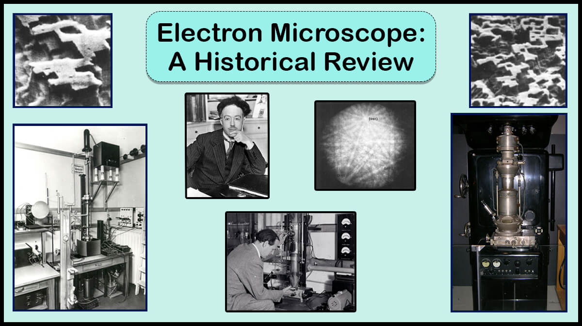
Invention History
The early prototype of the electron microscope was first developed in 1931 by Ernst Ruska and Max Knoll at Berlin Technical University, which was capable of four-hundred-power magnification. Then, Siemens financed the work of Ernst Ruska and Bodo von Borries to develop applications for the electron microscope, especially with biological specimens, and produced the first commercial electron microscope in 1938.
Current transmission electron microscopes remain based upon Ruska’s prototype, although, nowadays they are capable of two million-power magnification.
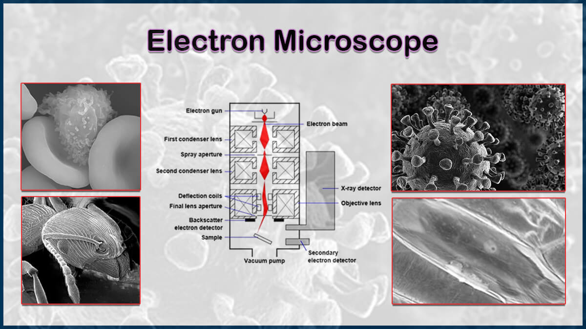
Different Parts of an Electron Microscope
Electron microscopes have several parts including:
- Electron gun generating electrons in different methods and provides electron beam incident on the specimen
- Electromagnetic lenses that help to focus the electron beam on the specimen and magnify the image
- Apertures, such as condenser or objective apertures, used to manipulate electron beam dimeter and focus to obtain high-resolution images
- Sample holder to fix the specimen
- Image viewing system to obtain the final image
Electron Interaction with Specimen
Different reactions may occur when a high-energy electron beam strikes a specimen. Some of the electrons collide with the specimen atoms and return in the opposite direction by changing their direction 180 degrees. These electrons are called backscattered electrons. A number of other electrons pass close to the atoms. Their path is so close to the specimen atoms that some of their energy is transferred to the electrons of the atom. As a result of this energy transfer, the incident electron loses some of its energy and changes direction, and the specimen atom loses its electron and ionizes.
The electron separated from the atom that leaves the atom with very little energy (about 5 electron volts) is called a secondary electron. Each of the incident electrons can produce several secondary electrons. The hole created in the atom is filled by electrons at a higher energy level due to the separation of the secondary electron. The descent of an electron to a lower energy layer causes excess energy in the atom. This excess energy is compensated by the separation of an electron from the outer layer of the atom or the emission of X-rays from the atom. The separated electron is called the auger electron (Figure 1).

If the thickness of the sample is small enough, a bunch of electrons passes through it without interaction. These electrons are called unscattered electrons. Some of the incident electrons also deflect elastically after colliding with an atom. That is, they pass through the sample in another direction without losing their energy. Electrons that undergo inelastic collision with the atoms also lose some of their energy and pass through other parts of the sample.
Types of Electron Microscopes
Types of electron microscopes include four main types:
- Transmission Electron Microscope (TEM)
- Scanning Electron Microscope (SEM) (SEM)
- Field Emission Scanning Electron Microscopy (FESEM)
- Reflection electron microscope (REM)
- Scanning tunneling microscopy (STM)


1- Transmission Electron Microscope
A transmission electron microscope is used to look at thin specimens (Tissue sections, molecules, etc.) through which electrons pass and produce an image. TEM is in many ways similar to a conventional light microscope. TEM is used to image intracellular space (In thin sections), the structure of protein molecules (Using the Metal Shadowing technique), the structure of molecules in viruses and skeletal filaments, and the arrangement of protein molecules in cell membranes.

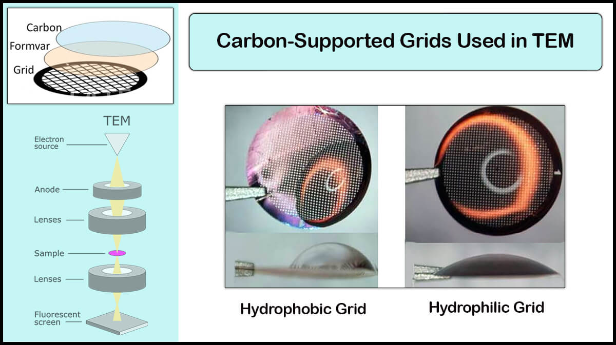
It works in two basic operation modes– imaging and diffraction modes, in the former an image of the sample is obtained, while the latter is a powerful tool for cell reconstruction and determination of crystal orientation.The specimen is often an ultrathin segment with a thickness of less than 100 nm or suspended on a grid with a standard size of 3.05 mm in diameter, and a thickness and mesh size ranging from a few to 100 μm, typically made of copper, molybdenum, gold or platinum.
2- Scanning Electron Microscope
Scanning electron microscopy is based on the emission of secondary electrons and backscattered electrons and reveals information on the sample including surface morphology, chemical composition, and crystalline structure of the sample. Since secondary electrons have low energy, they have a small mean free path in solid materials and move at the surface to a depth of a few nanometers.
 and relation of back scatting electrons intensities with the crystalline structure (right)")
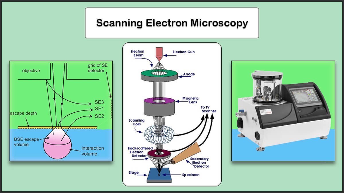

The image created by the secondary electrons is from the surface of the object with a resolution of less than 1 nanometer and is useful for illustrating the morphology and topography of the sample surface, while the image created by the backscattered electrons is deeper and has a lower resolution due to their higher energy, hence provides valuable insight in the samples with multi-phase composition.
The electron interactions with the sample generate x-rays that can be used for elemental mapping of the sample (EDS–Energy Dispersive X–ray Spectroscopy) but do not lead to volume loss of the sample, thus SEM imaging is known as a non-destructive method, and it is possible to analyze the sample several times. If you would like to read an overview of SEM and how it works, click the link below.

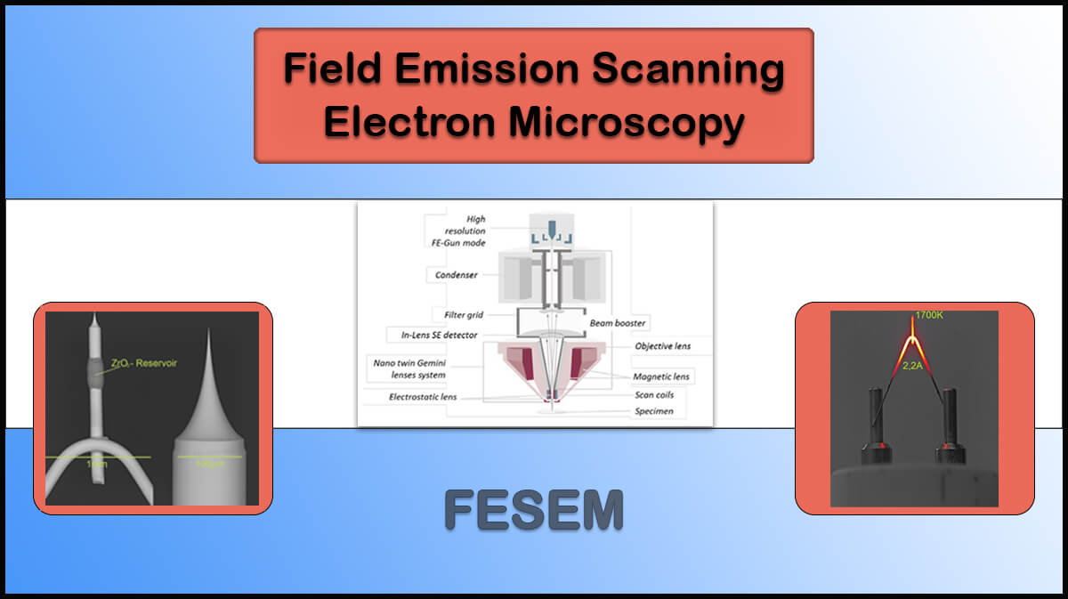
Field Emission Scanning Electron Microscopy (FESEM)
Field emission scanning electron microscopy (FESEM), an improved SEM variant, is mostly used when SEM fails to provide a sharp or appropriate morphology of a specified specimen.
In FESEM the electrons are generated through a field emission cathode with a narrower probing beam at low or high electron energies, which provides clearer, less electrostatically distorted images, enhanced spatial resolution down to 1.5 nanometers, and minimizes sample charging and damage. You can read more about FE SEM and difference between SEM and FE-SEM here …
3- Reflection Electron Microscope (REM)
In the reflection electron microscope (REM) an electron beam is incident on a surface identical to the previous methods, but rather than using the transmission (TEM) or secondary electrons (SEM), the reflected beam of elastically scattered electrons is detected. This technique is typically combined with other characterization methods like reflection high energy electron diffraction (RHEED), reflection high-energy loss spectroscopy (RHELS), and spin-polarized low-energy electron microscopy (SPLEEM), which is used for the investigation of the microstructure of magnetic domains.
Also REM data can be correlated with data from Auger electron microscopy (AES). Reflection electron microscopy (REM) is now an advanced technique to study the surface structure of crystals with a resolutions of better than 1 nm, in which clear images of surface steps with 0.1 to 0.2 nm height is accessible.

4- Scanning Tunneling Microscopy (STM)
STM is mainly used for imaging surfaces at the atomic level based on the concept of quantum tunneling. In STM, an extremely conductive tip is brought very close to the sample surface with a bias voltage applied between them, which allows the electrons to tunnel through the separating vacuum.
The resulting tunneling current provides a profile based on the tunneling probability of an electron from the tip to the sample since it is a function of distance, applied voltage, and the local density of states (LDOS) of the sample. This method can distinguish features smaller than 0.1 nm with a 0.01 nm (10 pm) depth resolution.

Specimens
Electron microscope specimens should be small enough to fit the sample holders perfectly. Specimens are usually mounted rigidly on the sample holder with an electrically conductive adhesive. If the specimen is electrically non-conductive or poorly conductive, electrical charges (especially secondary electrons) accumulate on it and interfere with the imaging of the sample when scanned by an electron beam.
For imaging the specimens with an electron microscope, they must be electrically conductive (at least at the surface) and electrically grounded to prevent any accumulation of charges on them.
Applications of Electron Microscopy
Electron microscopes are widely used to investigate the structure of an extensive range of biological samples and inorganic materials including micro-organisms, cells, large molecules, metals, and crystals.
In life sciences, electron microscopy is utilized to investigate the molecular nature and mechanisms of disease. Also, it enables the scientists to view the 3D structure of biological tissues or cells, verify the structure of proteins, and study viruses in a biological context.
In industry it is mainly used for quality control and failure analysis, also it is widely used whenever characterization of materials is needed in forensic science, mining, petrochemical, food science, etc.

Advantages of Electron Microscopes
- Exceptionally high magnification
- Extremely high resolution
- Provides investigation in a greater depth of field
Disadvantages of Electron Microscopes
- Electron microscopes are expensive to build and maintain
- They must be settled in stable buildings (sometimes underground) with special instruments such as magnetic field canceling systems
- The samples largely have to be viewed under vacuum conditions
- Observation of non-conductive materials requires conductive coating (gold/palladium alloy, carbon, osmium, etc.)
- Samples of hydrated materials, including almost all biological specimens, have to be prepared in various ways to become stabilized, also their thickness might be reduced by ultra-thin sectioning, and their electron optical contrast should increase through staining
Maintenance of an electron microscope imaging system
An electron microscope is a vacuum system that is sensitive to contaminations, so needs regular inspection to get the best result.
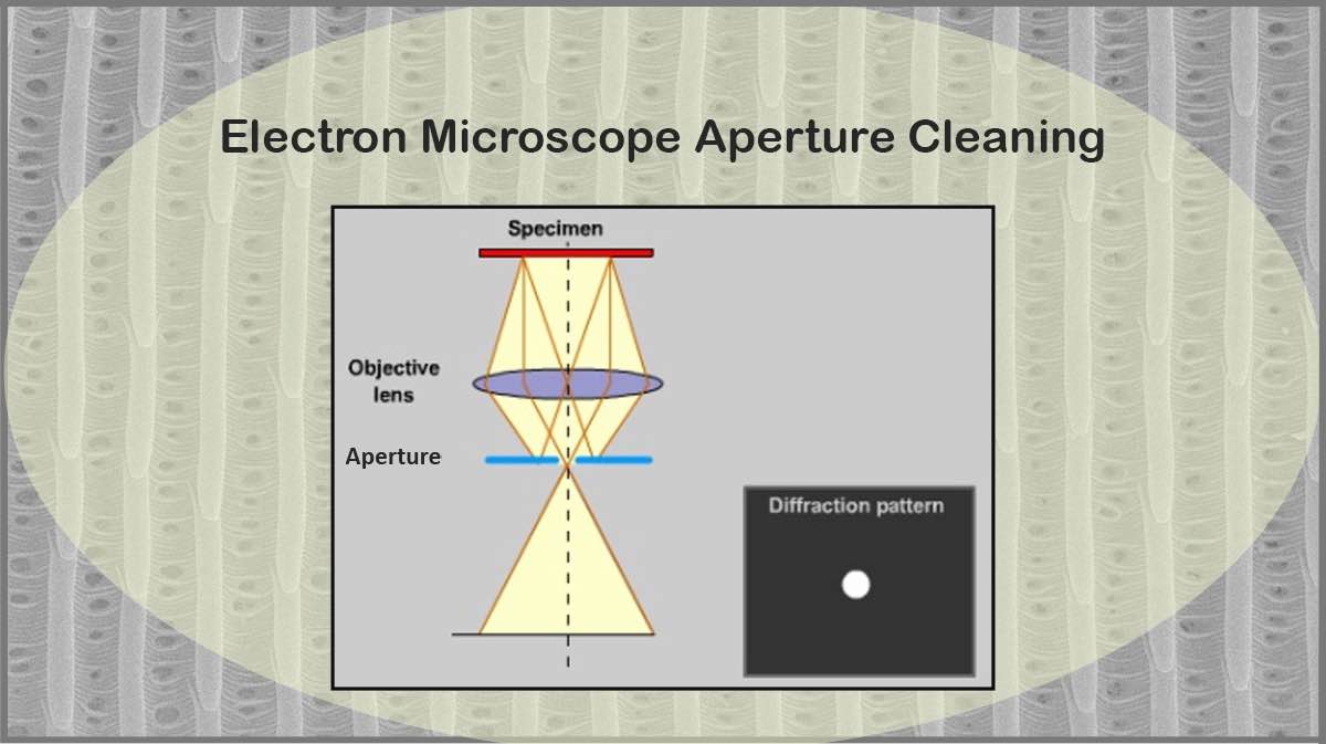
To prevent contaminations, the SEM chamber should be cleaned with a soft cloth and proper cleaning agents, like isopropyl alcohol or acetone, or a low-power hoover, to wipe the walls and the sample holder from dust, grease or other contaminants, regularly. The electron microscope aperture cleaning is usually performed by thermal evaporation of the contaminants on them, where Vac Coat thermal evaporators like DTE, DTT, and DSCT-T are helpful.
The contaminations can be source of outgassing, which is undesirable in a vacuum system. The mean free path of electron beam increases with decrease in the pressure level, resulting in less unwanted interactions of the electron beam on its path and obtaining high-quality images. So the vacuum chamber of an electron microscope should be checked for leakages to make sure it will reach the required vacuum level.
SEM calibration is a vital process that should be done with a standard sample with reproducible results, like metal nanoparticles, to check beam alignment, resolution, magnification, contrast, depth of field etc., to confirm the measurement accuracy.


Preparing an Electron Microscope Sample
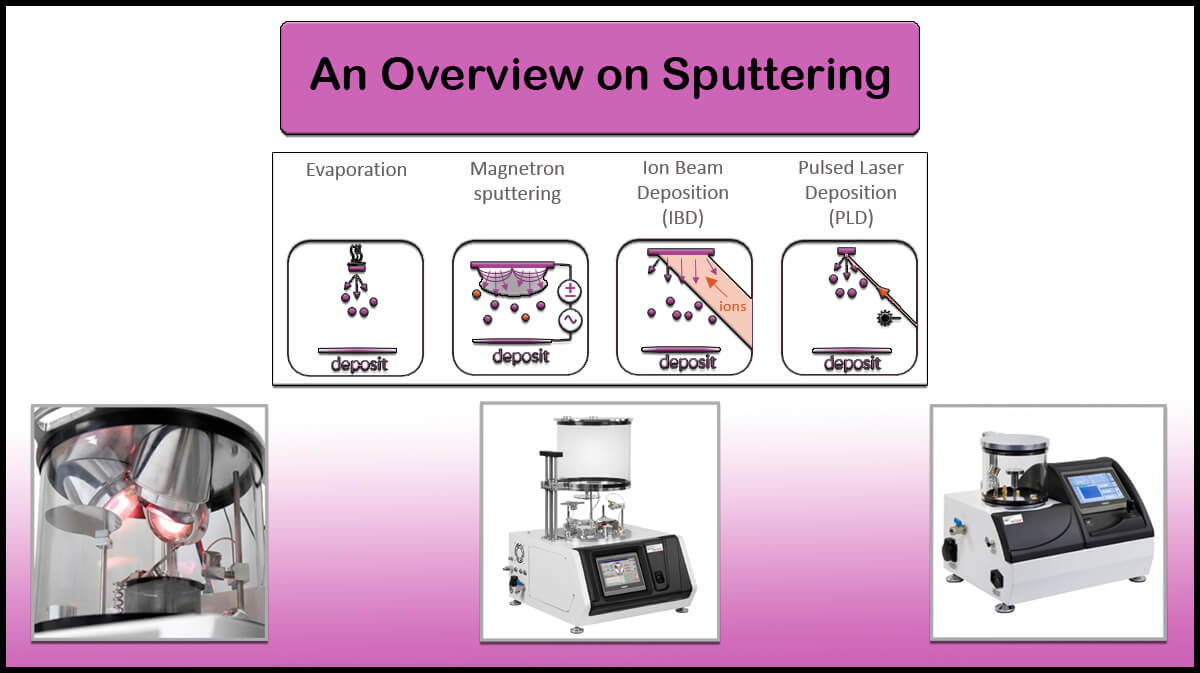
In the preparation stage, a very thin layer of several nanometers of conductive metals is usually coated on non-conductive or poorly-conductivity specimens using sputtering or thermal evaporation deposition methods, so they can withstand the high energy beam of electrons without evaporating or charging effects. The materials most often deposited are: carbon, gold, platinum, gold/palladium alloy, iridium and chromium.
In the sputtering method, the specimens are placed in a vacuum chamber and then in the presence of argon plasma, a thin film of nanometers of the target material is deposited on the specimen’s surface.
Electron Microscope Images
Here, some electron microscope images are displayed from various sources:
Figure 7. Images Obtained by Electron Microscopy from Different Samples: an Ant, Red Blood Cells and a Lymphocyte, and the Inner Surface of an Onion Flake
Vacuum Coating Systems and Electron Microscopy
Models of Vac Coat Ltd. systems that are capable of performing sputtering are suitable options for users of electron microscopes. Among the Vac Coat’s products, models of DSR1, DST1, DSCR, DSCT, and DST3 are suitable for sputtering, depending on the desired material (noble or oxidizing) the models equipped with just a rotary pump or the models equipped with rotary and turbomolecular pumps could be selected.
Also, DCR and DCT models are Vac coat carbon coaters equipped with rotary and turbo molecular pump suitable for SEM sample preparation as a SEM Coater.


The Thermal evaporation deposition method can also be used to prepare electron microscope specimens. In this method, the sample is placed in a vacuum chamber and then the vapor of the desired material, which is heated up by the electric current passing through it, coats the sample with a thin film of several nanometers. Thermal evaporation coating machine model DTT made by Vac Coat Ltd. is very suitable for this purpose.
The electro-evaporation method is also used to deposit carbon on electron microscope specimens. By passing a high electric current through a carbon fiber or carbon rod, the carbon evaporates in a vacuum chamber and deposits on the specimens. For more information about vacuum coating systems, refer to the Vac Coat site.

Some Of Vac Coat Products


References
- https://en.wikipedia.org/wiki/Electron_microscope
- https://serc.carleton.edu/research_education/geochemsheets/techniques/SEM.html
- https://www.jeol.co.jp/en/applications/pdf/sm/sem_atoz_all.pdf
- https://www.britannica.com/technology/scanning-electron-microscope
- https://www.nanoscience.com/techniques/scanning-electron-microscopy/
- https://en.wikipedia.org/wiki/Scanning_electron_microscope
- https://en.wikipedia.org/wiki/Scanning_tunneling_microscope
- https://en.wikipedia.org/wiki/Transmission_electron_microscopy
- https://en.wikipedia.org/wiki/Reflection_high-energy_electron_diffraction
- https://photometrics.net/field-emission-scanning-electron-microscopy-fesem
- https://www.dartmouth.edu/emlab/gallery/
- Cowley, J.M. (1988). Reflection Electron Microscopy. In: Howie, A., Valdrè, U. (eds) Surface and Interface Characterization by Electron Optical Methods. NATO ASI Series, vol 16. Springer, Boston, MA. https://doi.org/10.1007/978-1-4615-9537-3_9
- https://ems-microscopy.com/en/how-to-look-after-your-scanning-electron-microscope/
Hi VacCoat
How can we improve the quality of scanning electron microscope images?
With these items, you can improve the quality of scanning electron microscope images:
1- Having a smaller aperture so the electron probe diameter incident on the specimen is small, and we can see features of that order.
2- Increasing condenser lens current (CLC) results in focusing the electrons near the optical axis and restricts spreading of electron beam.
3- Lower the working distance to obtain higher resolution than in the case of higher working distance.
4- Increase beam energy to reduce the electron wavelength and hence better resolution. But this will cause the image on the screen to be a mixture of surface and sub-surface features.
5- Coating conductive materials with finer grain sizes like palladium on non-conducting sample to obtain higher resolution images.
Dear VacCoat
What is cryo-electron microscopy?
Cryo-Electron Microscopy (Cryo-EM) is a technique to preserve and protect the biological samples during observation by freezing them in a very cold liquid (like liquid nitrogen), imaging them close to their native state. Cryo‐EM is generally used to investigate the structure of biological macromolecules and macromolecular super complexes like chromosomes.
What is the range of voltages used to accelerate electrons in SEM and TEM?
For SEM imaging normally the accelerating voltage is in the range of 0.5-30 kV, whereas in TEM it is higher, since the electron should pass through the speciman and form an image. So TEM imaging needs a voltage in the range of 100-300 kV.
What is the resolution in electron microscope imaging?
The resolution of EM imaging strongly depends on the microscope structure and the electron wavelength, determined by the accelerating voltage. The higher the voltage, the fewer the wavelength, hence better resolution. The resolution is half of the detecting wavelength, so for a transmission electron microscope with an electron wavelength of about 4 picometers, it is about 2 picometers. But practically, the resolution is limited by the objective lens system to about 0.1 nm.
What type of samples can be viewed with an electron microscope?
Electron microscopes are ideal for viewing solid samples—both biological (e.g., cells, tissues) and non-biological (e.g., metals, polymers, semiconductors). Samples usually need to be dehydrated, fixed, and often coated with a conductive material (like gold or carbon) to improve image quality.
Why do samples need to be coated before SEM imaging?
Coating non-conductive samples with a thin metal or carbon film prevents charging under the electron beam, enhances signal strength, and improves image resolution. Vacuum coating systems, like sputter coaters and thermal evaporators, are typically used for this step.
What are the main types of electron microscopes?
“There are four primary types of electron microscopes:
Transmission Electron Microscope (TEM): Transmits electrons through a thin specimen to form detailed internal images.
Scanning Electron Microscope (SEM): Scans a focused electron beam across a specimen’s surface to produce detailed topographical images.
Reflection Electron Microscope (REM): Utilizes reflected electrons to study surface structures.
Scanning Transmission Electron Microscope (STEM): Combines TEM and SEM techniques, scanning a focused beam over a thin specimen and detecting transmitted electrons.”
What software is typically used for electron microscopy imaging?
Most modern systems come with proprietary imaging and analysis software for real-time image capture, 3D reconstruction, EDS (Energy-dispersive X-ray spectroscopy) integration, and measurement tools.
An incredibly comprehensive and well-structured explanation of the electron microscope this post captures both the depth of scientific detail and the clarity needed for true understanding. The comparison between electron and optical microscopes beautifully highlights the power of electron imaging, while the sections on TEM, SEM, FESEM, REM, and STM provide a complete perspective on their unique functions. The inclusion of applications, advantages, and maintenance tips makes it highly practical for researchers and students alike. A brilliant resource for anyone passionate about advanced microscopy and material science!