Thin Films coating and applications
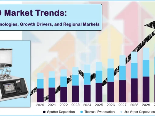
A thin film is a layer of material with a thickness in the range of a nanometer to a few micrometers. Many industries make use of different deposition methods to create thin films. Thin films are widely used in our everyday life, such as the metal coated glass used as mirror in every home. VacCoat as a manufacturer and designer of Vacuum Coating Systems, uses Physical Vapor Deposition (PVD) methods, such as sputtering, thermal evaporation, and pulsed laser deposition (PLD), to create different types of thin films.
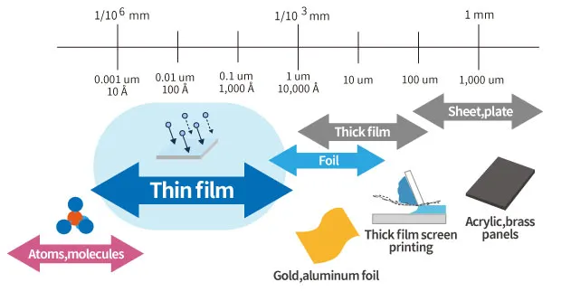
Why thin films are important?
Deposition of thin films on solids helps to improve their surface properties. In this manner, forming a thin film on a bulk material is used to obtain the desired mechanical, electrical or optical behaviors on the bulk material surface, thus achieving exceptional features such as higher conductivity, corrosion resistance, reflection, or hardness on the surface.
Thin films deposition process
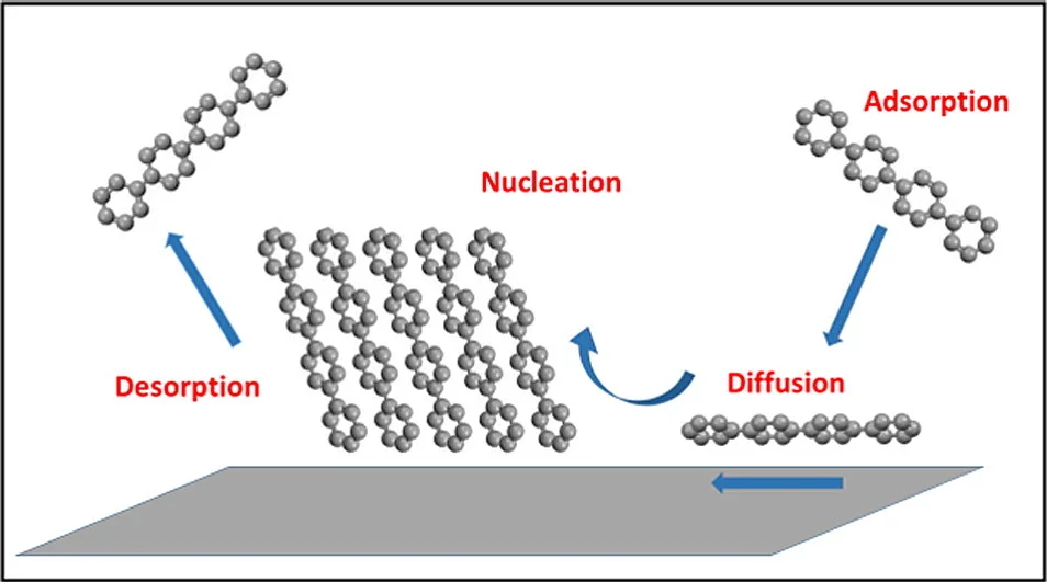
Deposition of thin films on a substrate has several phases, including adsorption, surface diffusion, and nucleation, each depending on the material and the substrate properties, and deposition method and parameters. The interactions between adsorbates and the substrate surface determines the growth mode and the structure of the resulting thin film.
Deposition Techniques
There are numerous deposition methods to create thin films of different materials on various substrates with innumerable structures. These methods are divided into two main category: Chemical and Physical methods.
- Chemical Deposition:
In chemical deposition, the reaction of a precursor fluid on the substrate results in the formation of a thin layer on the solid. Electroplating, sol-gel, dip coating, spin coating, chemical vapor deposition (CVD), plasma enhanced CVD (PECVD), and atomic layer deposition (ALD) are popular chemical deposition methods.
- Physical Deposition:
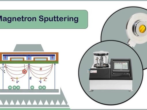
Physical deposition of a thin film is mainly achieved by deposition of the vapor of the material in a low-pressure environment, thus called physical vapor deposition (PVD). PVD method has a good accuracy and uniformity that has been highly regarded. Various techniques of sputtering, thermal evaporation, carbon coating, electron beam evaporation, molecular beam epitaxy (MBE), and pulsed laser deposition (PLD-T) are well-known of physical vapor deposition methods.
Thin Films Properties
Thin films have different optical, electrical, and mechanical properties compared to their bulk materials. Here is a brief description of these features:
- Electrical properties:
Electrical properties of a thin film depends on the film material (metal, semiconductor, or insulator) and the substrate. However, one of the main factors effecting the electrical conductivity is the size effect. Charge carriers inside a thin film have shorter mean free path compared to the bulk material, which in conjunction with more scattering points like structural defects and grain boundaries, results in reduced electrical conductivity.
- Optical properties:
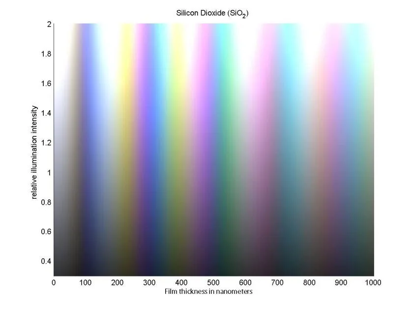
The optical properties of materials is determined by their optical coefficients like refractive index and extinction coefficient. These parameters are affected by electrical conductivity of the material, so due to the previous section, optical properties of thin films is connected to the structural defects and features like voids, localized defects, and oxide bonds. In case of thin films, the transmission and reflection coefficients are highly dependent on the film roughness and thickness.
- Mechanical properties:
Thin films mechanical properties show dependence on film’s thickness and microstructure, emerging a different behavior as compared to their bulk form. The stored stress in the thin film during the deposition process and later on, especially in physical vapor deposition methods, improves its mechanical properties such as yield strength and hardness. The existence of microstructures like grain boundaries, dopants, and dislocations in the thin films results in larger hardness compared to their bulk counterparts.
Thin Films Characterization Techniques
- Chemical composition determination:
The elemental composition of thin films can be studied through ion scattering techniques like Rutherford backscattering spectroscopy (RBS) or spectroscopic techniques such as X-ray photoelectron spectroscopy (XPS).
- Morphology and structure:
The crystalline structure and microstructures can be characterized by various methods like X-ray diffraction (XRD) and Raman spectroscopy. The thin film morphology is mainly investigated by field emission-scanning electron microscopy (FE-SEM), transmission electron microscopy (TEM), and atomic force microscopy (AFM).
- Thickness measurement:
Thin film thickness can be measured during and after the deposition by various techniques like quartz crystal microbalance (QCM) sensors, ellipsometry, profilometry, and interferometry.
Thin Films Types and Applications
Improvement of a lot of industries in the last century is due to the development of thin films and their deposition methods. These industries include semiconductor electronics, magnetic recording media, integrated circuits, LEDs, optical coatings (such as anti-reflective coatings), hard coatings in order to protect tools, pharmaceuticals, medicine and many other industries. Thin films have several applications in various fields; furthermore, they play a significant role in the study and development of materials with unique and special properties, such as the superlattices which make it possible to study quantum phenomena.
Types of thin films, due to the thin films properties, can be categorized as follows:
- Optical thin films: Used to create reflective coatings, anti-reflective coatings, solar cells, monitors, waveguides and optical detector arrays
- Electrical or electronic thin films: Used to make insulators, conductors, semiconductor devices, integrated circuits and piezoelectric drives
- Magnetic thin films: Usually used to make memory disks
- Chemical thin films: They are used to create resistance to alloying, diffusion, corrosion and oxidation, as well as to make gas and liquid sensors
- Mechanical thin films: Tribological coatings to protect against abrasion, increase hardness and adhesion and use of micro-mechanical properties
- Thermal thin films: They are used to create insulation layers and heat sinks
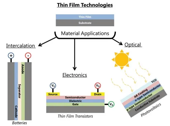
Also, they have many applications in industry and research including decorative coatings, biosensors, plasmonic devices, photovoltaic cells, batteries, and acoustic wave resonators.
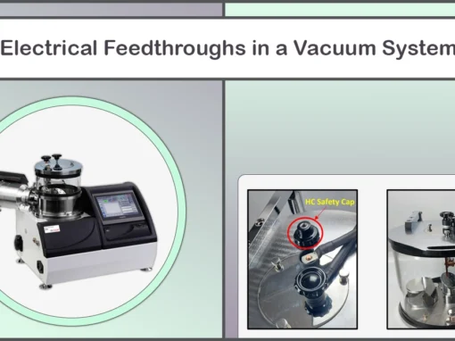
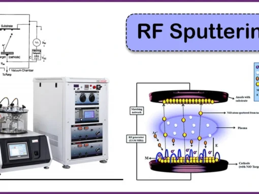
VacCoat Vacuum Coating systems (such as Desk Sputter Coater – DSR1 and Desk Thermal Evaporator – DTT) are all used to create thin films by physical vapor deposition (PVD). They divide into four categories, sputter coaters, carbon coaters, thermal evaporators, and PLD systems. VacCoat triple cathode desk sputter coater with thermal evaporator (DST3-T) performs both sputtering and thermal evaporation. Model DST3-A with angled cathode is able to do confocal sputtering of three target. RF sputtering is also available for non-conducting targets. Model DST3-S with straight cathodes can uniformly deposit large samples up to 8 inches. For more information, visit vaccoat.com.
References
- Benelmekki, M., & Erbe, A. (2019). Nanostructured thin films–background, preparation and relation to the technological revolution of the 21st century. Nanostructured Thin Films, 1–34. doi:10.1016/b978-0-08-102572-7.00001-5
- https://www.susumu.co.jp/usa/tech/highfrequencychip02.php
- Rao, M. C., and M. S. Shekhawat. "A brief survey on basic properties of thin films for device application." International Journal of Modern Physics: Conference Series. Vol. 22. World Scientific Publishing Company, 2013.
- https://en.wikipedia.org/wiki/Thin_film
- Frey, Hartmut. "Applications and developments of thin film technology." Handbook of Thin-Film Technology (2015): 1-3.
- Winkler, Adolf. "Initial stages of organic film growth characterized by thermal desorption spectroscopy." Surface science 643 (2016): 124-137.
- Acosta, Edwin. "Thin films/properties and applications." Thin Films. IntechOpen, 2021.
- https://www.soapbubble.dk/en/articles/thin-film-interference