What is SEM and When it Invented?
Scanning electron microscopy is an efficient and non-destructive technique that provides detailed information on the morphology, composition and structure of the studied materials. The first scanning electron microscope was invented in 1942. It was shown at that time that Secondary Electrons (SE) produced topographic contrast using the collector positive bias rather than the sample. After that, many changes were made until the first commercial sample of scanning electron microscope was introduced in 1965.
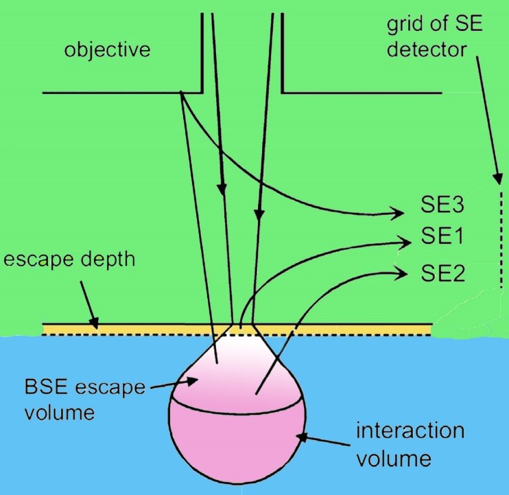
In scanning electron microscopy (SEM), two classes of electrons are detected: secondary electrons (SE) and backscattered electrons (BSE). Backscattered electrons are the redirected electrons of the elastically collided electron beam with the sample, where secondary electrons originate from the sample atoms and result from the inelastic collision of the electron beam with the sample with less energy than backscattered electrons.
As a result of the inelastic collision of the electron beam with the sample surface, the energy of the electron beam electrons is transferred to the conduction band electrons and sometimes the valence band of the sample which separates these electrons from the sample atom, which is called secondary electrons. BSEs return from deeper points of the sample and depend on the atomic number of the material, the larger the atomic number, the material appears in the brighter image. The SEs are sampled from the more superficial areas and provide a lot of surface detail information. As a result, these two groups of electrons carry different information (Figure 1).
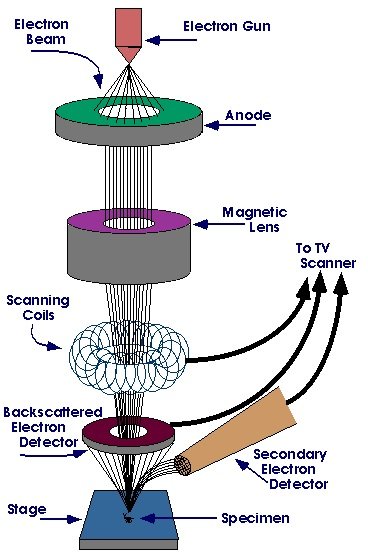
A scanning electron microscope consists of several parts:
- An electron source,
- Electromagnetic lenses that focus the generated electron beam on the specimen,
- SEM stub, on which the specimen is mounted,
- Electron detector,
- And image processing facilities.
Electron source
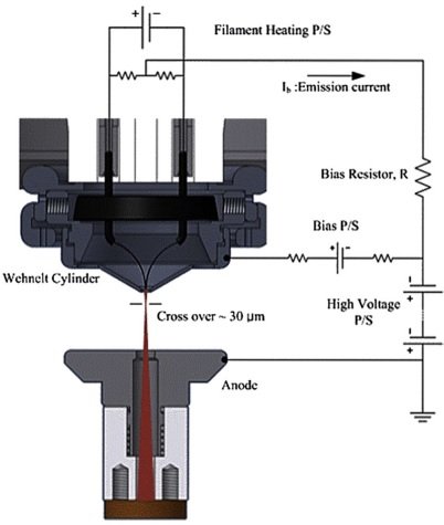
The electron source in SEM have been improved since its invention. In conventional electron microscopy the electrons are separated from the filament by resistively heating the tungsten filament and the anode accelerates the electron beam after leaving the thermionic source. The tungsten electron filament, with a diameter of about 100 mm, is the most common types of electron source mainly due to its low price point, high reliability, and suitability for low magnification imaging. Owing to the thermionic emission of the heated tungsten, the electrons spread to a wide trajectory from the source.
Electromagnetic lenses
The electron beam with the energy ranging from 0.2 keV to 40 keV, is focused onto a spot about 0.4 nm to 5 nm in diameter by one or two condenser lenses. The beam goes through pairs of scanning coils or deflector plates placed in the final lens, which bend the beam in the x and y axes so that it can scan over a rectangular area on the sample surface.
Sample preparation
In the case of samples that are not electrically conductive, such as dielectrics and semiconductor materials, a sample preparation process is required prior to imaging. Due to the collision of the electron beam in the imaging process using electron microscopy, the non-conductive structure of these specimens traps electrons on the surface of the material and thus causes the surface to temporarily become charged. This phenomenon causes white areas appearing in the image captured by the electron microscope. The conductive layer deposited on the sample prior to the microscopic process acts as a channel and eliminates the charges created on the sample surface.
Also, the presence of a conductive layer on the sample stimulates secondary electrons, especially at the surface. A conductive coating is appropriate when the topographic features of the specimens are not significantly enlarged or hidden. The selected material must have a suitable secondary electron emission coefficient to help improve image contrast.
The optimum thin film conditions for coating scanning electron microscopy specimens are obtained when the thin film is of minimum thickness (0.5 to 3 nm) and contains fine grain size so in addition to removing the excess electrical charges on the sample, it also improves contrast in low-density materials. Moreover, conductive layer grains should have low surface mobility, such that they do not affect the sample appearance, and be smaller than the probe diameter.
Field Emission Scanning Electron Microscopy (FE-SEM)
With the advancement of the technology and the advent of Field Emission Scanning Electron Microscopes (FE-SEM), higher resolution images became available. The method of operation of these microscopes is similar to that of conventional scanning electron microscopes (SEM), in which the surface is scanned by an electron beam. The biggest difference between SEM and FE-SEM is the electron generation system. FE-SEMs use field electron emission guns. These guns concentrate low-energy and high-energy electrons at a low electrical potential (about 0.02 to 5 kV) and increasedspatial resolution, which prevents contaminating the sample surface since does not require thermal energy to overcome the surface potential.
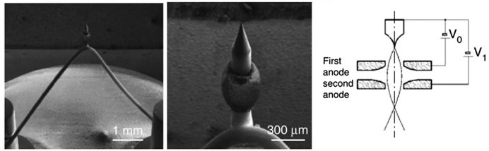
Field Emission Guns (FEG)
Field emission guns in FESEM imaging are divided into three types:
- Cold field emission (CFE) source
In CFEs the electron emission functions at room temperature and depends only on the electric field applied between the electrodes, using tungsten single crystal emitters. Although the current of the emitted electron beam is low, high brightness can be achieved due to the small diameter of the electron beam and emission area. This kind of FEG requires high vacuum condition to operate, otherwise, after a long operation period, adsorbed gas molecules on the FE-SEM tip will form a layer and can result in unstable current emission.
- Thermal field emission (TFE) source
TFE guns operate at high temperature (1800K), which minimizes the adsorption of gas molecules on the gun tip and the stability of electron emission is improved even in lower vacuum conditions.
- Schottky emission (SC) source
SC has a larger electron sources compared to CFE at similar supplied energy, which enabled SC guns to prevent vibrations. This guns can utilize emitters of tungsten single crystals coated in zirconium oxide.
FESEM vs. SEM: benefits and limitations
- Thermionic emission of the electrons result in the substrate contamination, not occurring in the field emission electron sources.
- In the SEM method, a resolution of 3-7 nm is achievable, while in the FE-SEM the resolution is 1.5 nm or better.
- The conductive layer coated on a sample to be subsequently imaged by FE-SEM must be very thin and uniform and have finer grain size compared to what is required for SEM imaging.
- Better contrast in low-density materials imaging through FE-SEM technique is possible.
- In FE-SEM, the electron source requires higher vacuum environment (higher than 10-9 Torr) during operation to ensure electron stability and prevent contamination of the cathode.
- FE-SEM electron sources suffer low beam current stability.
VacCoat SEM sputter and carbon coaters provide conductive layer deposition for SEM and FESEM sample preparation equipped with rotary pump (DSR1, DSCR) for low vacuum and Turbomolecular pump (DST1, DSCT) for high vacuum deposition.
VacCoat also offers DST3-T sputtering system plus thermal deposition with Turbomolecular pump to deposit composite layers of several materials. This coating system with the optional RF generator and plasma cleaner can provide deposition of a wide range of conducting and semi-conducting materials.
References
[1] Abd Mutalib, M., et al. "Scanning electron microscopy (SEM) and energy-dispersive X-ray (EDX) spectroscopy." Membrane characterization. Elsevier, 2017. 161-179.
[2] https://sites.google.com/site/quantummechanics16/home/electron-microscope
[3] https://www.microtonano.com/TIN-Target-material-selection-for-coating-SEM-samples-using-an-SEM-sputter-coater.php
[4] https://blog.phenom-world.com/sem-electrons
[5] https://en.wikipedia.org/wiki/Scanning_electron_microscope