Sputtering Process
Sputtering in physics is called to the process in which a plasma of high energy particles/ions knock out the species on the surface layer of a solid target. This phenomenon naturally happens in the outer space, constantly forming the universe and causes spacecraft’s corrosion. Here, on Earth, the science and industry make use of sputtering process to generate or eradicate thin films of nano/micrometer thickness for various applications in optics, electronics, etc.
What is Sputtering?
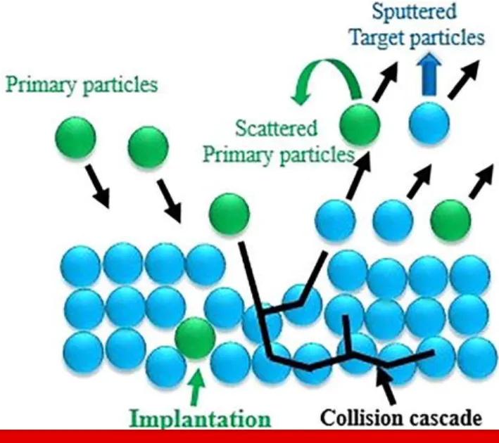
Due to the collision of high-energy ions with the target material atoms, momentum transfer occurs between them. These ions, called incident ions, cause a series of collision cascades on the surface of the target. Sometimes these successive collisions cause the ions to travel long distances and lose their energy. If the ion energy at the time of reaching the target surface is greater than the bonding energy between the atoms of the target material, the collided atom separates from the target material. This phenomenon is called Sputtering.
Sputter Yield
The energy of sputtered atoms varies widely, and usually the kinetic energy of these atoms is more than tens of electron volts (typically 600 eV). Approximately one percent of the ions that hit the surface of the target material have a ballistic impact and return to the substrate, causing Re-sputtering. The average number of atoms ejected from the surface of the target material by the collision of each ion is called the Sputter Yield.
The sputter yield depends on many factors, such as:
Plasma gas pressure
The angle at which the ions strike the surface of the target material
The amount of ion energy during the collision
The weight of the ions
The weight of the atoms of the target material
The binding energy between the atoms of the target material
Magnetic field strength and design factors (in magnetron cathodes)
| Target Material | Density (g.cm-3) | Sputtering Yield |
| Au | 19.31 | 2.8 |
| Ag | 10.5 | 3.4 |
| Cu | 8.92 | 2.3 |
| Fe | 7.86 | 1.3 |
| C | 2.25 | 0.2 |
A table of sputtering yields of several material is displayed in Table 1. The numbers vary under different deposition conditions as mentioned earlier, but are useful for comparison purposes.
If the structure of the target material is crystalline, the orientation of the crystal axis relative to the surface is also an important factor in the sputtering yield.
Deposition
One of the applications of sputtering phenomenon is Deposition. Sputtering deposition is a method of creating thin films of a few nanometers to a few micrometers on the desired substrate. In this process, the atoms separated from the surface of the target material are gaseous. These thermodynamically unstable atoms tend to be on a surface in a vacuum chamber. The atoms on the substrate which form a layer with a few nanometers to a few micrometers thick, is called a Thin Film.
Physical Vacuum Deposition Method
This type of deposition is a physical vacuum deposition method (Physical Vapor Deposition). PVD is a set of deposition methods in which the material enters the vapor phase from the dense state and returns to the dense phase as a thin film.
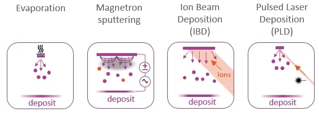
These vacuum deposition methods include three stages:
- Evaporation of the target material
- Transfer of vapor from the target material to the substrate
- Formation of a thin film on the substrate with accumulation of vapor of the target material
Sputtering Process
In order to vacuum coating by sputtering technology, ions need to be fired at the target material in the plasma medium. The gas to be used in the sputtering process must have two properties: first, that its atomic weight must be such that it can affect the atom of the target material, and second, it must not chemically react with the target material. According to the mentioned cases, the gases used in the Sputtering Process are from the group of noble gases in the last column of the periodic table (Argon, Xenon, etc.). Argon gas is the most common gas used in this process.
Gaseous plasma is a dynamic environment in which neutral gas atoms, ions, electrons, and photons are in near equilibrium. Since the plasma energy is transferred to the surrounding area a DC or RF power source should be used to form a sustainable plasma. Plasma is formed by injecting a noble gas (usually Argon) into a vacuumed chamber until it reaches a certain pressure (maximum 0.1 Torr), and applying DC or RF voltage.
- Sputtering rate
Sputtering rate is the number of monolayers per second sputtered from the surface of a target. It depends on the sputter yield (S), Molar weight of the target (M), material density (p), and ion current density (j), as represented in Equation (1):
Sputtering rate = (MSj)/(pNAe)
Where NA is the Avogadro number and e is the electron charge.
GLAD Sputtering
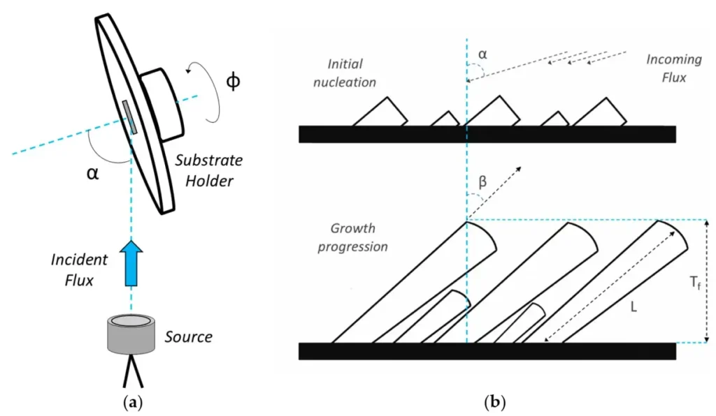
GLAD (Glancing Angle Deposition) sputtering is used in the deposition of microstructures mainly designed for optical devices. In this method various columnar or spiral nano/micro structures can be created by means of setting different substrate tilt angles and rotation speeds against the target.
VacCoat sputter coaters include substrate stages that are designed to tilt and rotate to perform GLAD sputtering.
Ion Beam Sputtering (IBS)
In this method the target atoms are sputtered by a focused high energy ion beam. The Argon ions are generated and accelerated inside a low vacuum ion source and leave it toward the target in a high vacuum environment (about 10-4Torr), with a pressure lower than what is required in a typical sputtering process chamber. This method allows sputtering deposition under lower impurity condition.
Ion Assisted Sputtering (IAD)
This method, which is an upgraded IBS method, makes the reactive sputtering possible by applying a secondary ion source directed onto the substrate. With introduction of non-inert gases like O2 and N2 and a second plasma formation, the sputtered target atoms react with the plasma and layers of metal oxide/nitride are deposited on the substrate.
Diode Sputtering
In diode sputtering, an electric potential difference is applied between the target and the substrate to form a plasma discharge inside a low vacuum chamber. The free electrons in the plasma are immediately removed from the negative potential electrode (cathode). These accelerating electrons collide with neutral gas atoms (Argon) in their path, causing the electrons in the shell of these atoms to separate. As a result, the gas atoms become positive ions and accelerate towards the cathode, causing the sputtering phenomenon. Glow discharge occurs when some of the positive ions return to their ground state by adsorbing free electrons and releasing photons.
This mechanism is called Diode Sputtering and the applied voltage can be DC (with constant poles) or RF (with alternating poles), depending on the target material. One of the problems with this method is that its coating rate is low and it takes longer to do the coating, which causes the target to heat up and damage its atomic structure, which is improved utilizing Magnetron Cathodes.
Magnetron Sputtering
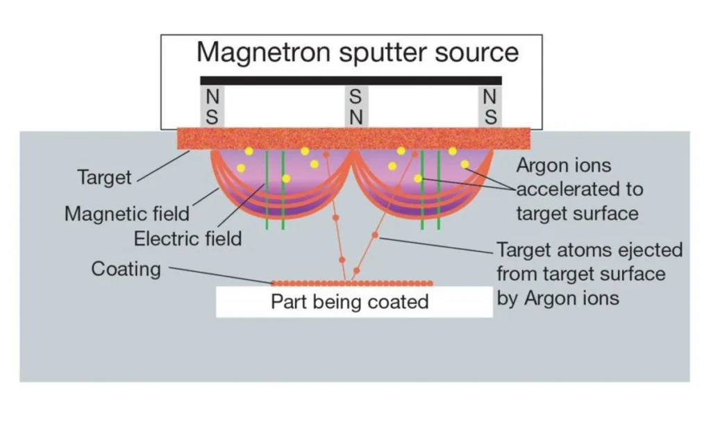
With the advent of magnetron sputtering method, the problems for diode sputtering were solved. By placing a number of magnets behind the cathode, the free electrons are trapped in the generated magnetic field just near the target surface. These electrons do not reach the substrate like the diode sputtering method and do not bombard the substrate surface.
The movement of these electrons in the path of the curve led by the magnetic field increases the probability of ionization of the neutral gas atoms many times over. Increasing the ions that hit the surface of the target intensifies the rate of deposition.
VacCoat is a designer and manufacturer of PVD systems that most products use magnetron sputtering methods, such as Desk Sputter Coater (DSR1), and Magnetron Sputter Coater (DST1-170 and DST1-300).
In addition, Vac Coat produces hybrid systems like Sputter Coater and Thermal Evaporator (DST3-Tand DST3), Sputter and Carbon Coater (DSCR, DSCT, DSCR-300, and DSCT), which are equipped with magnets behind the cathode and perform magnetron sputtering.
Both Diode and Magnetron sputtering methods can be performed with DC or AC (radio frequency, RF) voltages, depending on the target material.
- DC Sputtering
DC Sputtering is suitable for metals and materials that are electrically conductive. The DC power supply used in this method is less complex and more controllable than other power supplies, and has a lower manufacturing cost.
This is why DC sputtering is the most popular sputtering method in terms of power supply. The Desk Sputter Coater (DSR1) made by VacCoat Ltd. is a simple system that has a lower price than other models. This device is only capable of DC sputtering.
- RF Sputtering
In RF Sputtering an alternative voltage, with a frequency in the range of radio waves, is applied to the cathode instead of the DC voltage used in a typical DC sputtering. This results in continuous changing of negative/positive pole that prevents charge accumulation on the surface of insulating targets. With this technique, magnetron sputtering of non-conducting is made possible, and arcing plasma during deposition is avoided.
VacCoat sputtering systems like high-vacuum single-target sputter coater (DST1-300) and triple-target sputter coater (DST3) with thermal evaporator (DST3-T) are equipped with 600W DC power supply, 300 W RF power supply (optional) with auto matching box. Also, these models are supplied with a plasma cleaning option to clean substrate surfaces through plasma treatment.
The DST3-T, Triple Target Turbo Pumped Sputter Coater, is a multi-vacuum coater system that combines thermal evaporator and sputter coater in one single compact desktop system. The high vacuum system is suitable for deposition of a wide range of materials.
These high vacuum sputtering systems can deposit a wide range of target materials, including metals, metal-oxides, semiconductors, and ceramics on different surfaces for various thin film applications and FESEM sample preparation. For more information, you can see RF Sputtering post and if you are interested in types of electron microscopes, follow the links below.
- Confocal Sputtering
If the deposition process is performed from several cathodes, the Confocal Sputtering Technique can be used. In this technique, the cathodes are arranged in a circular pattern with a focal point. By placing the substrate that rotates around its axis at or around the cathodes focal point, a layer is deposited that has a much better uniformity than the layer deposited using a cathode. Also, this technique is effective to perform the deposition of several different materials simultaneously for alloying (Co-Sputtering) or asynchronous to create multi-layers.
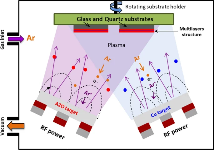
Using this technique, a uniform layer can be obtained on a substrate with a diameter twice the diameter of the target. Also, for materials that have low sputtering yield, the deposition can be applied using several cathodes simultaneously at a higher speed. The Triple Target Sputter Coater manufactured by VacCoat Ltd. models DST3-A and DST3-TA equipped with three angled and focal cathodes, are able to perform Confocal Sputtering.
- Reactive Sputtering
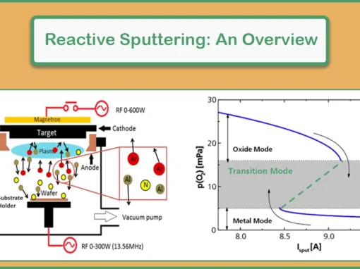
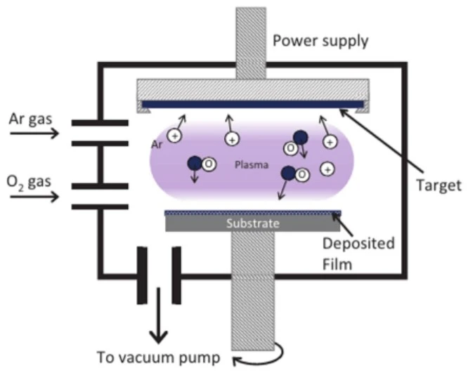
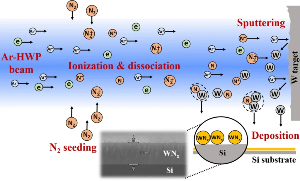
In this type of sputtering, the atoms separated from the target undergo a chemical reaction before being deposited on the substrate. The resulting deposited thin film will have a different composition than the target material composition. Chemical reaction occurs between the atoms separated from the target and reactive gases (such as Oxygen or Nitrogen) that enter the vacuum chamber during the deposition process.
By adjusting the amount of inlet gases and noble gas (Argon) used in this process, a thin film with the desired composition and stoichiometry can be deposited. The Vac Coat company has various models of Vacuum Coating Systems, such as DST1, DST3, and DSCR, with one or more inlets installed for reactive gas flow into the vacuum chamber during the deposition process.
High Power Impulse Magnetron Sputtering (HIPIMS)
HIPIMS is a new Magnetron Sputtering Method that uses high power pulses to increase target ionization. Compared to conventional magnetron sputtering, this method ionized atoms reach the substrate with more energy, which increases the density and quality of the deposited thin film.
High-Target-Utilization Sputtering (HiTUS)
The gaseous plasma can be generated in a chamber other than the main one and then introduced and guided to the target in the deposition chamber by DC electromagnets. This method has the advantage of uniform corrosion of the target during sputtering process, which results in higher target utilization of near 95% compared to a typical DC/RF sputtering.
Vac Coat is the manufacturer of a wide range of PVD systems, employing sputter coating technology to achieve nanometer thin films for a variety of applications.
Vac Coat produces various models of Vacuum Coating Systems to perform Sputtering Deposition Process. These systems are classified into different models depending on the ultimate pressure they can reach, the power supply used in them for the sputtering process, the number of cathodes, the dimensions of the vacuum chamber etc. For more information about VacCoat Ltd. products, please visit vaccoat.com.
Reference
- http://www.ajaint.com/what-is-sputtering.html
- http://www.semicore.com/what-is-sputtering
- https://en.wikipedia.org/wiki/Sputter_deposition
- https://www.angstromsciences.com/sputtering-yields
- Bundesmann, Carsten, and Horst Neumann. "Tutorial: The systematics of ion beam sputtering for deposition of thin films with tailored properties." Journal of Applied Physics 124.23 (2018): 231102.
- https://polygonphysics.com/applications/ion-beam-sputter-deposition/
- Bairagi, Samiran, et al. "Glancing angle deposition and growth mechanism of inclined AlN nanostructures using reactive magnetron sputtering." Coatings 10.8 (2020): 768.
- https://www.specs-group.com/fileadmin/user_upload/products/technical-note/sputter-info.pdf
- https://www.horiba.com/int/scientific/applications/material-sciences/pages/gdoes-the-analytical-companion-tool-for-magnetron-sputtering-deposition/
- https://ebrary.net/191961/engineering/reactive_sputtering
- Tiwari, Atul. Handbook of antimicrobial coatings. Elsevier, 2017.
- Doghmane, N. E. A., et al. "Confocal magnetron sputtering deposition of Cu/AZO bilayer structures: effect of Cu thickness on microstructural and optoelectronic properties." Journal of Materials Science: Materials in Electronics (2022): 1-11.
- Ghazal, H., & Sohail, N. (2022). Sputtering Deposition. Thin Film Deposition - Fundamentals, Processes, and Applications [Working Title]. doi: 10.5772/intechopen.107353
- WNx thin film-Huang, Tianyuan, et al. Sputter deposition of WNx thin films by helicon-wave-excited argon plasma with N2 seeding. Surface and Coatings Technology 410 (2021) 126941.