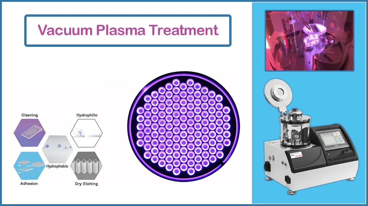
Plasma created by glow discharge can be manipulated to treat surface areas to achieve desired surface properties for various applications.
Precision Vacuum Coating Solutions for Advanced Thin-Film Applications

Plasma created by glow discharge can be manipulated to treat surface areas to achieve desired surface properties for various applications.
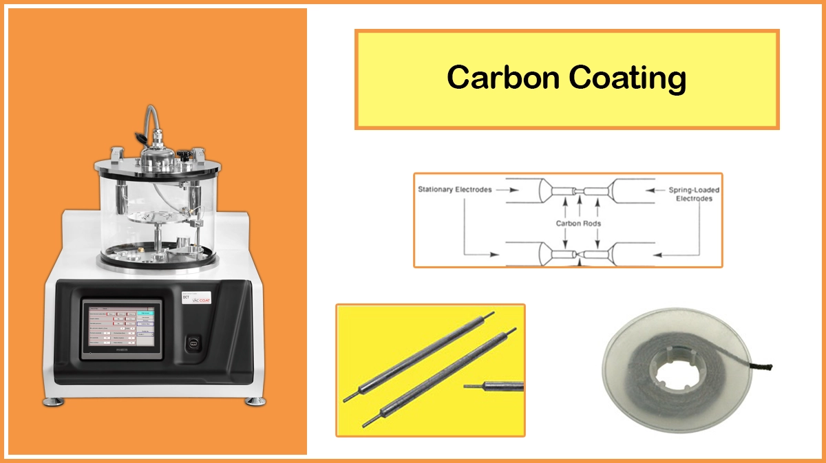
Carbon coating is a thin layer of carbon that be coated by various methods, like thermal evaporation, E-beam deposition, or sputter coating and utilized in different applications.
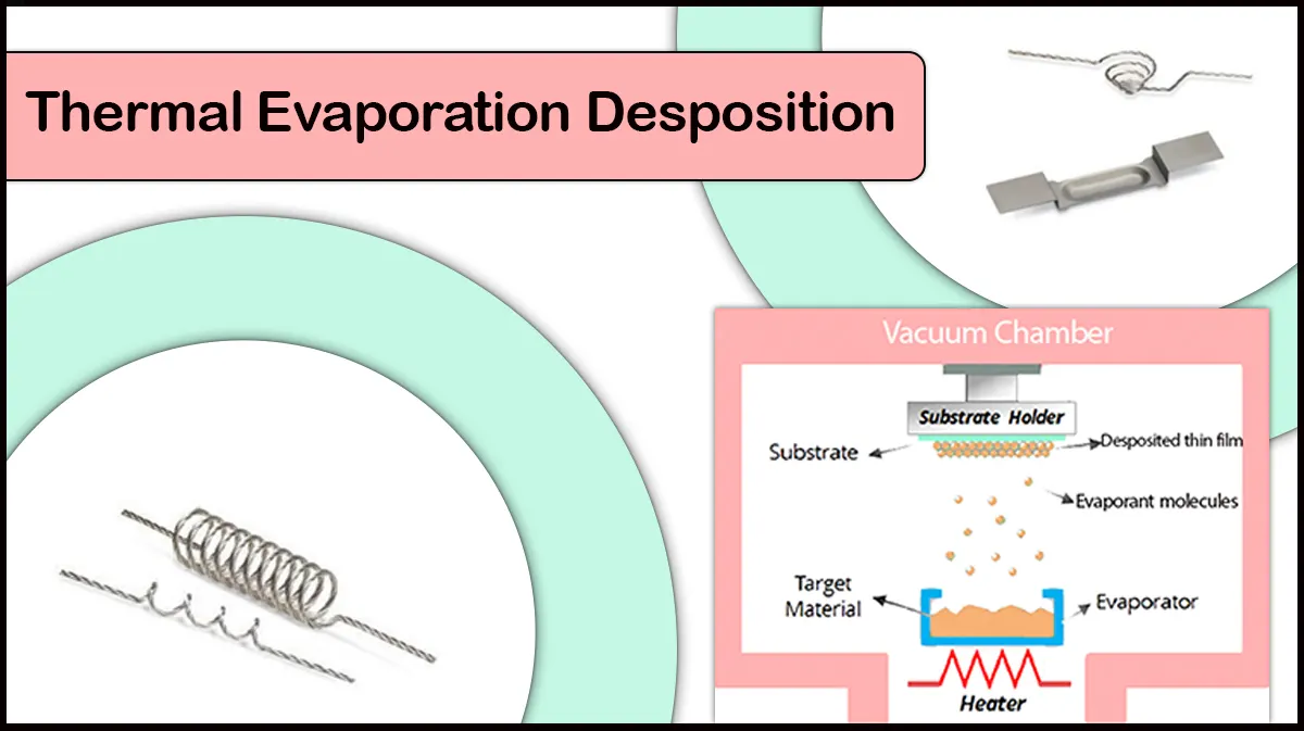
Thermal evaporation deposition technique is widely used as a straight method of forming thin films for various applications like solar cells and sensors.
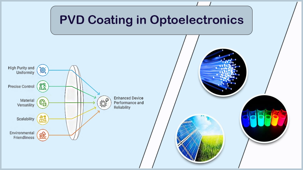
PVD coatings in optoelectronics enable high-purity, uniform thin films of metals and ceramics for various functions, including forming interconnects, barriers, and insulators, used in LEDs and ICs.
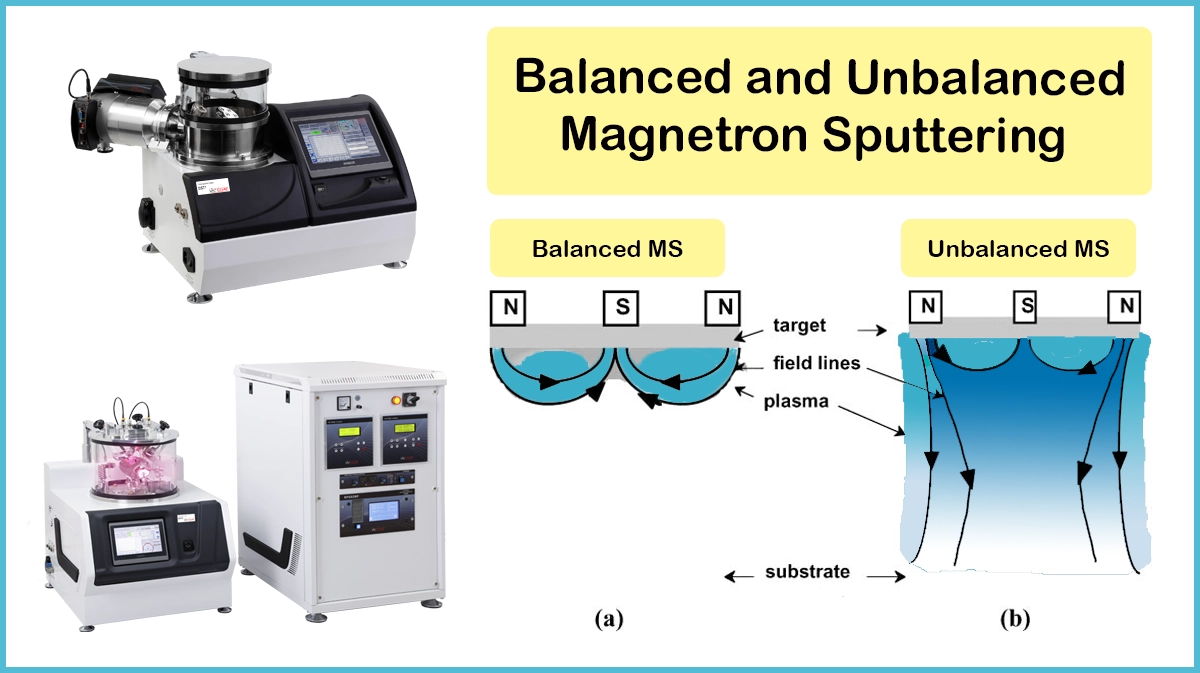
The use of Magnetron Sputtering is done in two ways that relates to the configuration of the magnets. Balanced magnetron sputtering: If all the magnets have the same power.
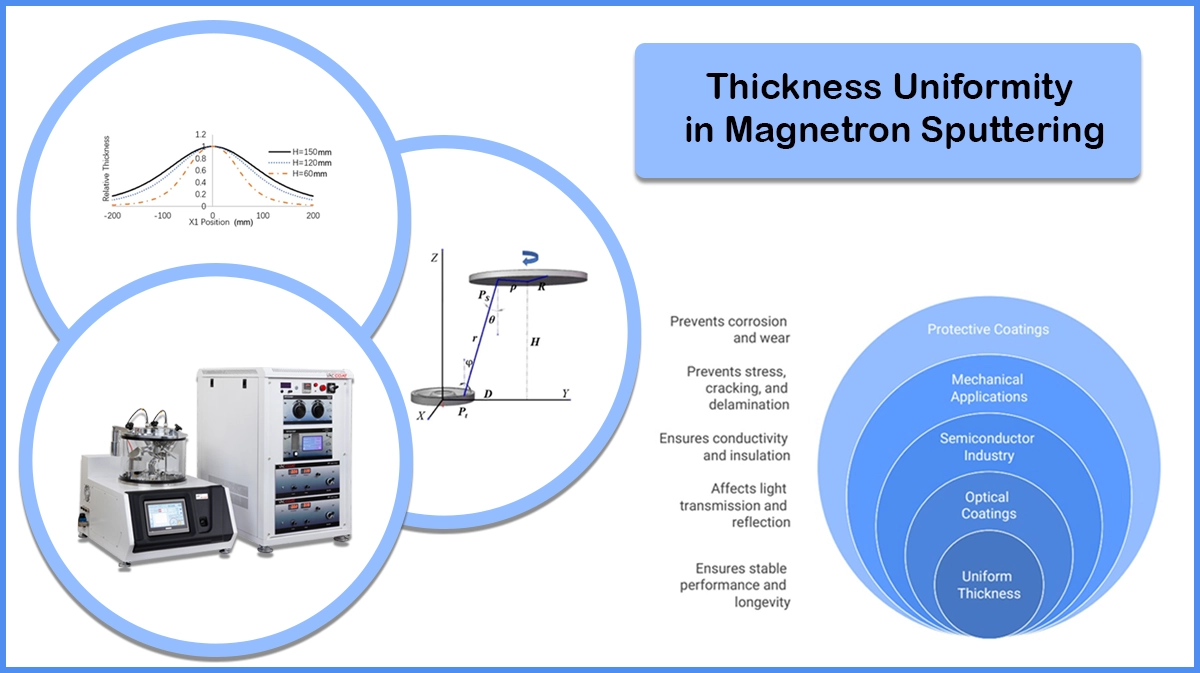
Thickness uniformity of thin films is an important feature in a coating performance that can be manipulated through adjusting deposition chamber geometrical factors.
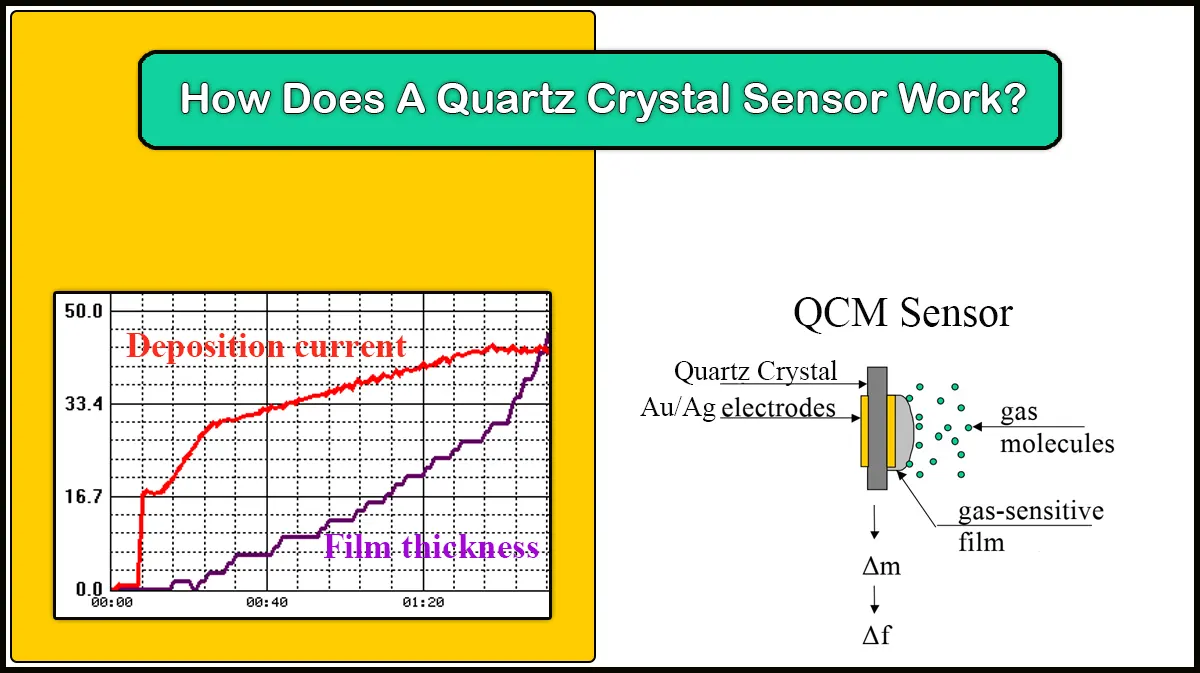
A quartz crystal microbalance (QCM) sensor is a piezoelectric crystal that detects the extra mass placed on it based on the change in its resonating frequency.
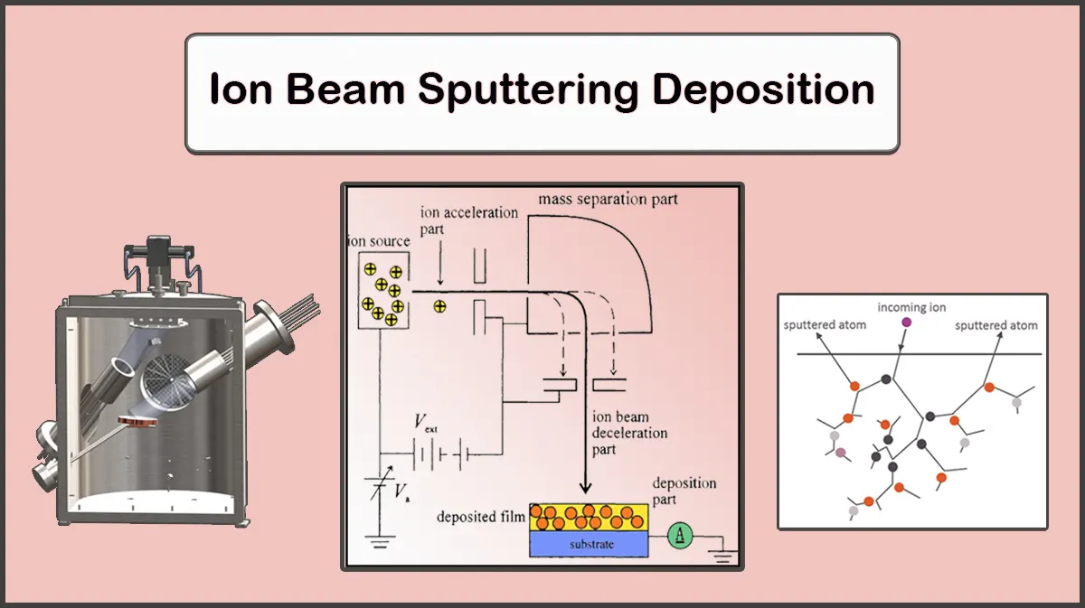
Ion Beam Sputtering Deposition is one of the favorable methods to form high purity, uniform, and dense thin films resulting from energetic ion sputtering of the target material.
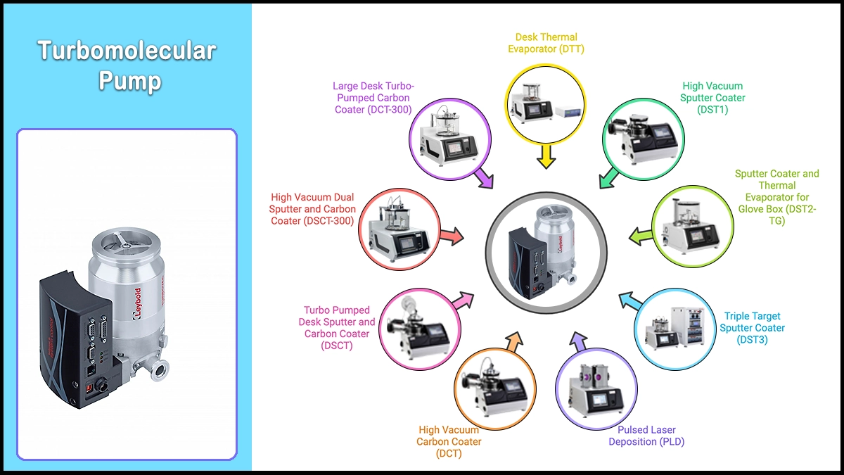
Turbomolecular pumps can be used in the range of rough vacuum, high vacuum, and ultra-high vacuum with a constant pumping speed of up to 4000 lit/s.
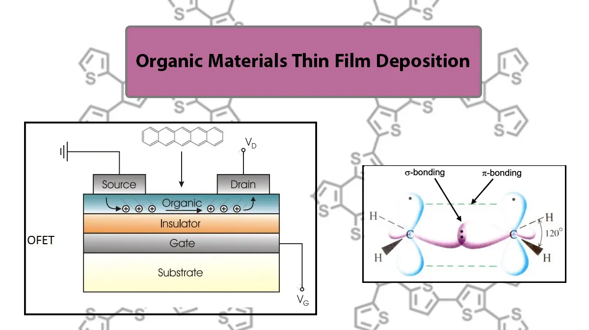
Organic materials play an important role in development of electronic and electro-optic devices due to their electronic band structure, low cost, and high flexibility.
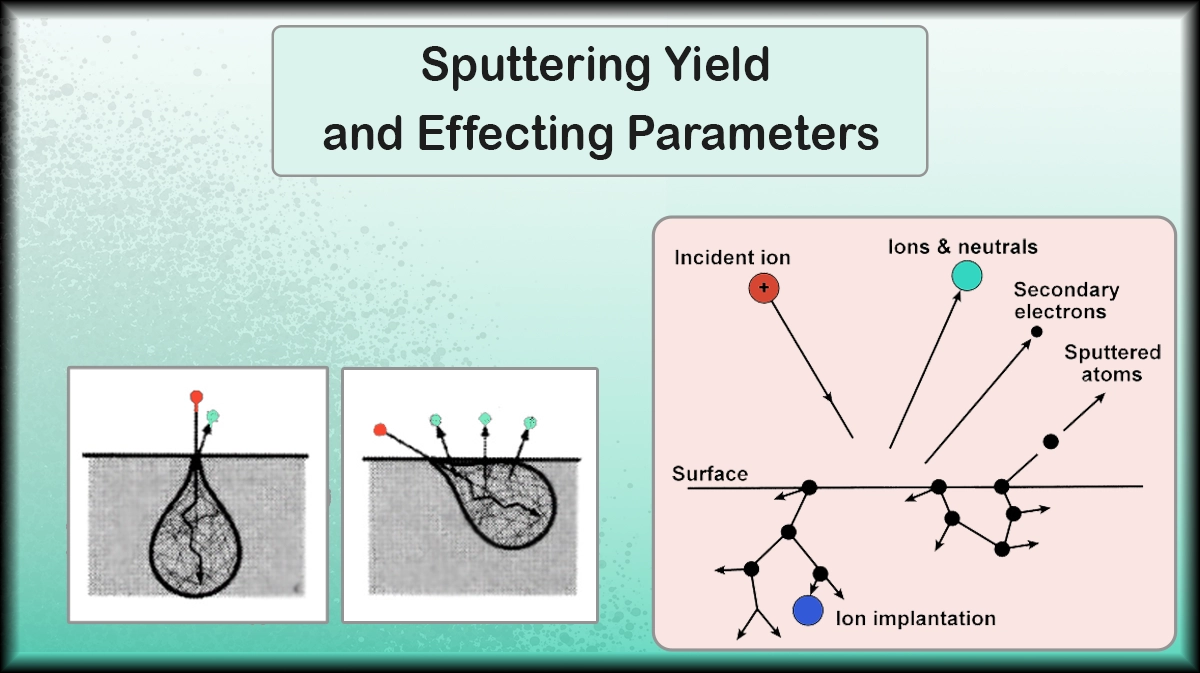
Sputter yield is a key parameter in the sputter coating process that highly affects the sputtering efficiency and the deposition rate and is a function of several factors, including energy and target material.
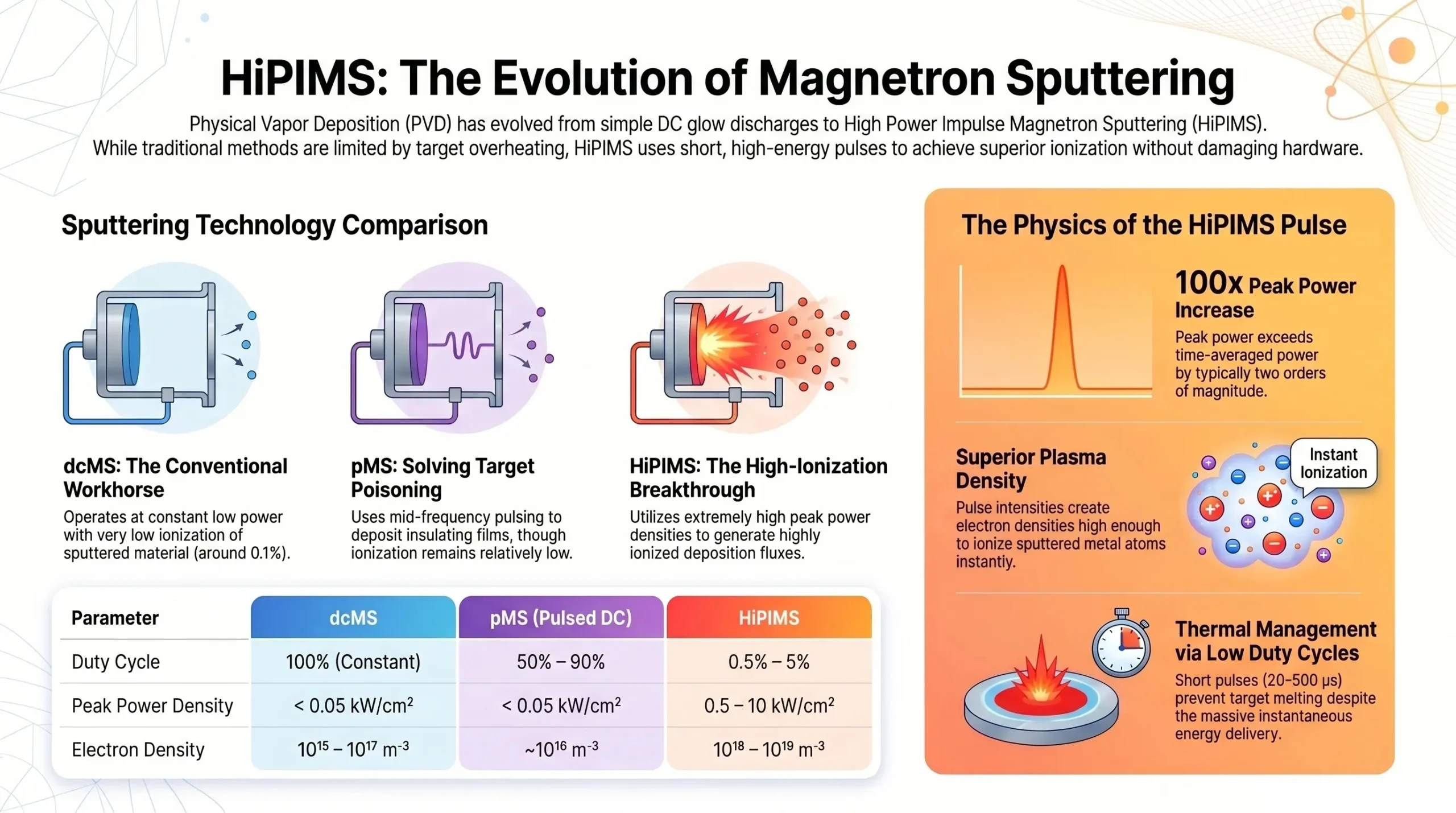
HIPIMS method uses low duration, high-power pulses to generate highly ionised plasma for enhanced mechanical features in PVD coatings.