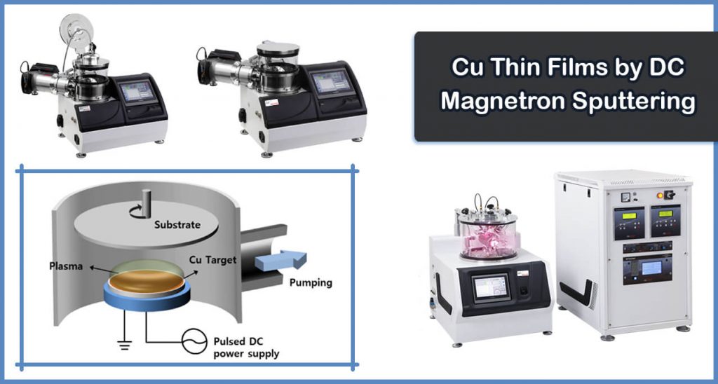
Electrically Conductive Cu Thin Films by DC Magnetron Sputtering
Many studies focus on the growth of copper microstructure as a function of the coating method. The increase of resistivity of copper thin films is due to various phenomena such as scattering from defects (vacancies, dislocations, grain boundaries) and also scattering from the free surface, bottom interface, and side-wall interfaces of the films. In this way, the mean free path of electrons decreases, which leads to an increase in resistance.
In this regard, the size of the crystallite plays a key role for a polycrystalline film because the concentration of defects is proportional to the number of crystallite boundaries that act as trap centers.
As the film thickness decreases, the size of the crystallite, as well as the mobility of the charge carriers, decreases. The presence of a significant amount of amorphous phase (when the films are not well crystallized) leads to the expansion of crystallite boundaries, which, according to Slater’s theory, increases the height of the energy barrier across the crystal boundaries. The results of DC Magnetron Sputtering of copper thin films with different coating film parameters have been investigated.
The main purpose of the studies was to determine the effect of coating time, target-substrate distance, DC voltage, sputtering power, and argon gas pressure on the morphology and grain size of copper thin films. According to Figure 1, studies have shown that the size of the crystals in different coating methods has a significant effect on the final electrical resistance of the coated layer. The SFCD stands for supercritical fluid chemical deposition.
In one study it was observed that the thickness of the deposited layer increases with increasing deposition voltage while the surface roughness decreases. For example, for a glass substrate of 30 x 20 mm2 in the target to the substrate distance of 30 mm during the sputtering time of 5 minutes, by changing the sputtering voltage from 600 to 1200 volts, a film with a thickness of 300 nm can be obtained at the sputtering voltage of 1000 volts.
The copper coated reached a resistance of 1.9 microns per centimeter close to the value of copper bulk resistance. The results show that as the DC voltage increases, the surface roughness decreases and the structure of the Cu thin film reaches a better crystallinity, Figure (2).
In another study, the effect of argon gas pressure on the quality of the deposited copper thin film was investigated. In this study, the DC voltage was set at 400 volts, the target and substrate distance at 100 mm, and the deposition current between 69 and 200 mA. The results of this study indicate that increasing the argon pressure from 0.5 to 1.5 Pa increases the resistance. This is due to the increase in the rate of the thin film coating and thus the reduction in the size of the copper crystallites in the final Cu thin films.
Sputtering power has a significant effect on nucleation and growth of copper thin films by magnetron sputtering. According to the diagrams in Figure 3, copper coated films at higher sputtering power showed better crystallinity and lower electrical resistance than copper thin films coated at lower sputtering power. Considering the nucleation and growth of Cu thin films in the initial stage of magnetron sputtering, it has been found that the progress of nucleation and growth of Cu thin film in higher power sputtering is much faster than lower sputtering power.
In this study, copper films were deposited on Si (100) thin films at a distance of 80 mm from the substrate for 10 minutes with different sputtering powers in the range of 0.55 to 2.74 Wcm-2 using DC magnetron sputtering. Copper coated with high sputtering power of 2.74 Wcm-2 showed better crystallinity and lower electrical resistance than copper thin films coated with low sputtering power of 0.55 Wcm-2.
Better adhesion of the deposited films on the substrate is achieved in lower current value and longer time of copper deposition. According to the diagrams in Figure 4, the increase of current value/time of Cu deposition and decrease of target-substrate distance increase the grain size. Studies have shown that resistance is constant for films thicker than 250 nm copper, and greater thickness has no effect on changing electrical resistance.
Vac Coat Sputter Coaters
Vac Coat Ltd. is known for designing and manufacturing high-quality and reliable Physical Vapor Deposition and vacuum coating systems. Its products include sputtering systems, carbon coating systems, thermal evaporation, and pulsed laser deposition. All VacCoat Sputter Coaters are able to deposition by magnetron sputtering method and some of them can create Cu thin films by DC Magnetron Sputtering.
The Sputter Coaters include sputter coater with a thermal evaporator (DST3 & DST3-T), magnetron desk sputter coater (DST1-300 & DST1-170), and turbo pumped desk sputter and carbon coater (DSCT & DSCT-T), that equipped by Turbomolecular Pump. For more information, visit the website please.
References
- Baptiste Giroire, Mohamed Ali Ahmad, Guillaume Aubert, Lionel Teulé-Gay, Dominique Michau, et al. A comparative study of copper thin films deposited using magnetron sputtering and supercritical fluid deposition techniques. Thin Solid Films, Elsevier, 2017, 643, pp.53-59. ff10.1016/j.tsf.2017.09.002ff. ffhal-01652547.
- Govind Panwar, Lalit Thakur, Development of Electrically Conductive Copper Thin Film by using DC Magnetron Sputtering Process, IJERT, RDME – 2018 (Volume 06 – Issue 16).
- https://dokumen.tips/documents/structural-and-electrical-properties-of-cu-films-deposited-on-glass-by-dc-magnetron.html
- Minh-Tung Le, Yong-Un Sohn, Jae-Won Lim and Good-Sun Choi, Effect of Sputtering Power on the Nucleation and Growth of Cu Films deposited by Magnetron Sputtering, Materials Transactions, Vol. 51, No. 1 (2010) pp. 116 to 120.
- MECH, R. KOWALIK, P. ŻABIŃSKI, Cu thin films deposited by dc magnetron sputtering for contact surfaces on electronic components, archivesofmetallurgyandmaterials, Volume 56 2011 Issue 4, DOI: 10.2478/v10172-011-0099-4.
- http://www.microlabgallery.com/gallery/1%20order%201.aspx
- Arun Augustin, K. Rajendra Udupa, Udaya Bhat K., Effect of Pre-Zinc Coating on the Properties and Structure of DC Magnetron Sputtered Copper Thin Film on Aluminium, American Journal of Materials Science 2015, 5(3C): 58-61,DOI: 10.5923/c.materials.201502.12.
- https://www.semanticscholar.org/paper/Residual-stress-control-of-Cu-film-deposited-using-Kim-Lee/e772d3be05e680e8623ad6d1e08d859bccac571e

