What is Superconductivity?
Superconductivity is a unique physical phenomenon manifested in certain materials. When cooled below a certain temperature, known as the superconducting transition temperature, such material exhibits exactly zero electrical resistance.
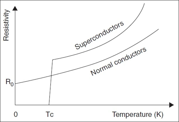
In conventional conductors, electrical resistance decreases gradually as the material is cooled, owing to the reduction of thermally induced lattice vibrations that scatter conduction electrons. However, as can be seen in the next figure, their resistivity converges to a non-zero value as the temperature approaches absolute zero (−273°C). Superconductors differ from normal conductors in that their electrical resistance plunges almost abruptly from a finite value to exactly zero at a specific point, the critical temperature (TC).
A Brief History of Superconductors and Superconductive Materials
Superconductivity was discovered unintentionally in 1911 by Heike Kamerlingh Onnes. While studying the properties of purified mercury at low temperatures, using liquefied helium, he observed that the electrical resistance of mercury abruptly vanished at approximately 4.2 Kelvin. Following this discovery, the family of superconducting materials gradually expanded to include other metallic elements such as lead and niobium (see figure 2), all with TC below 10 K. These materials are now broadly classified as Low-Temperature Superconductors (LTS), and their microscopic behavior can be explained by BCS theory, which describes how electrons form bound pairs known as Cooper pairs through interactions with lattice vibrations.
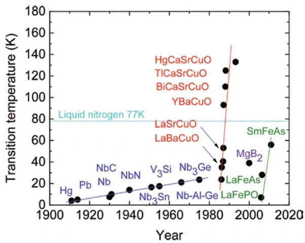
As illustrated in the previous figure, a revolutionary breakthrough came in 1986 when Bednorz and Müller discovered superconductivity in a copper-oxide ceramic compound (so called cuprate) at a temperature significantly higher than any previously known material. This new class of materials, which cannot be explained by the conventional BCS theory, have critical temperatures greater than the boiling point of liquid nitrogen (77 K) and they are termed High-Temperature Superconductors (HTS).
Nowadays, superconductivity is not just a laboratory curiosity; it has attracted significant attention from both researchers and industrialists. This is due to several reasons: their fascinating properties, the lowered cooling costs enabled by HTS materials, and the ability to fabricate superconductors in various forms—most notably thin films (which enable the exploration of superconducting phenomena and properties with small size and weight).
Properties and Characteristics of Superconductors
· Critical Parameters:
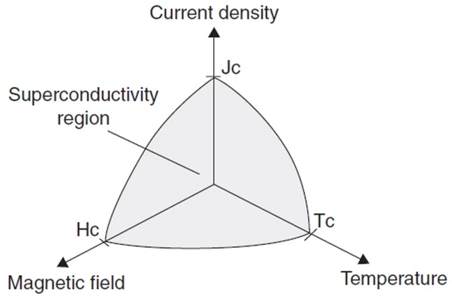
The most important feature of a superconductor is its critical temperature, or TC. However, the superconducting state is not defined by temperature alone, it is also bounded by two other critical limits represented by critical magnetic field (HC) and critical current density (JC). These three parameters are dependent on each other, for instance, cooling a superconductor further below its TC enables it to withstand higher HC and JC. The following figure illustrates the interplay of these three parameters that forms a phase boundary within which true superconductivity exists.
· Zero Resistivity
The most distinctive property of superconductors is zero electrical resistivity, though it should be noted that this is only valid when a direct current (DC) is conducted. This means an electrical current, once initiated within a closed superconducting loop, can circulate indefinitely without any energy dissipation.
· Perfect Diamagnetism
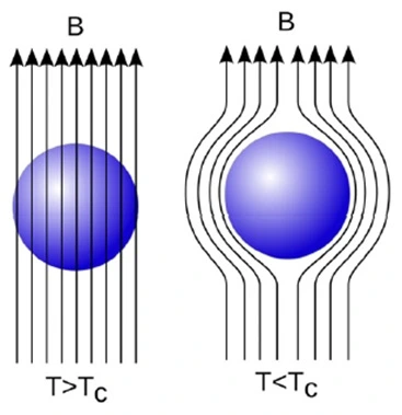
Another defining property of superconductors is perfect diamagnetism, also known as the Meissner effect. When an external magnetic field is applied to a superconductor, non-decaying screening currents are induced on the surface of the superconducting material which creates an opposing magnetic field preventing flux from penetrating inside the superconductor. As a result, the internal magnetic induction becomes exactly zero, making the superconductor a perfect diamagnet (see next figure). It is the Meissner effect that leads to the fascinating phenomenon of magnetic levitation of a superconductor.
· Quench
A superconductor quench refers to the sudden transition of a material from its superconducting state to the normal resistive state. This process is triggered when any one of the three critical parameters is locally exceeded. As a consequence, the affected area develops electrical resistance and generates a large amount of joule heating which in return accelerates the quenching process. While this positive feedback mechanism is usually regarded as a design challenge, it can also be useful for some applications. For example, superconducting fault current limiters (SFCLs) rely on this very property.
Classifications and Applications of Superconductors
There are many classifications for superconductors according to their properties and characteristics. We have already encountered the distinction between LTS and HTS superconductors. Another categorization, based on their interaction with an external magnetic field, divides them into Type I and Type II superconductors. A further, more practical classification is based on the physical form of the material, including bulk, wire, tape, thin film, etc.
The choice of geometry for a superconductor is driven by the specific demands of each application. Geometries like wire, tape, cylinder, … are used in wide applications such as SFCLs, magnetic resonance imaging (MRI) devices. However, in some applications, like maglev trains, energy storage, electrical motors and generators the bulk superconductors are preferred. On the other hand, superconducting thin films are the cornerstone of many high-tech applications including quantum computers, Josephson junctions, SQUIDs, and single-photon detectors.
Superconducting Thin Film Deposition Methods
In the fabrication and deposition of superconducting thin films, several important factors must be considered:
- Thin film quality
- Compositional homogeneity
- Uniformity
- Conformality
- Substrate compatibility
- Large area deposition
- Film thickness
A wide range of superconducting thin film deposition techniques had been developed and successfully applied long before the emerging need for superconductor films. The process characteristics of these conventional techniques are well understood, and this knowledge can be leveraged for the production of superconducting thin films. Among them, the most widely used fabrication processes can be categorized into:
- Solution-Based Deposition Methods
- Spin coating
- Dip coating
- Spray pyrolysis
- Chemical Vapor Deposition (CVD)
- Atomic Layer Deposition (ALD)
- Physical Vapor Deposition (PVD)
- Sputtering
- Thermal Evaporation
- Pulsed Laser Deposition (PLD)
- Molecular Beam Epitaxy (MBE)
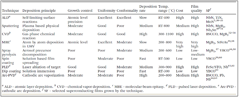
Besides the inherent benefits and drawbacks of each process, the deposition of superconducting thin films (particularly HTS) creates problems of its own. The following table provides a comparison of the existing superconducting thin films’ deposition techniques.
Practical Considerations for Deposition of Superconducting Thin-Film
The selection of a thin-film deposition technology depends on several factors, including film quality, thickness control, uniformity, conformality, deposition rate, substrate geometry, scalability, equipment cost, and process complexity. Different deposition techniques offer distinct advantages and limitations depending on the final application.
Superconductive Thin Films Deposition by PVD methods
Physical Vapor Deposition (PVD) encompasses several vacuum-based techniques, including magnetron sputtering, thermal evaporation, electron-beam evaporation, Molecular Beam Epitaxy (MBE), and Pulsed Laser Deposition (PLD).
These techniques are widely used for deposition of metals, alloys, compounds, functional materials, optical coatings, semiconductor structures, and superconducting thin films through physical processes.
Sputtering and PLD for Superconducting Thin Films
PLD
Pulsed Laser Deposition (PLD) uses a high-energy laser pulse to ablate material from a solid target, generating a plasma plume that deposits onto a substrate. PLD can produce high-quality films and is particularly useful for complex oxides, superconductors, and research materials where maintaining the target composition during deposition is important. Compared with MBE, PLD can offer a comparatively compact experimental configuration, although the process still requires a suitable vacuum chamber, laser system, and appropriate process control.
Sputter Coating of Superconducting Thin Films
Sputter deposition is one of the most versatile and widely used approaches for producing high-quality thin films. In sputtering, energetic ions generated in a plasma bombard a solid target, ejecting atoms from its surface. These atoms subsequently travel through the vacuum environment and condense on the substrate to form a thin film.
Modern sputtering technologies, particularly magnetron sputtering, provide excellent control over deposition parameters and can produce dense, uniform, and reproducible coatings of a wide range of materials, including metals, alloys, conductive compounds, and many oxides and other functional materials.
Magnetron sputtering also offers several practical advantages for research and industrial applications. It can operate at relatively low substrate temperatures, supports a broad range of substrate geometries, and can be configured for DC, RF, reactive, co-sputtering, and multilayer deposition. These capabilities make sputtering suitable for applications ranging from electron microscopy sample preparation to semiconductor research, energy materials, optical coatings, and advanced functional thin films.
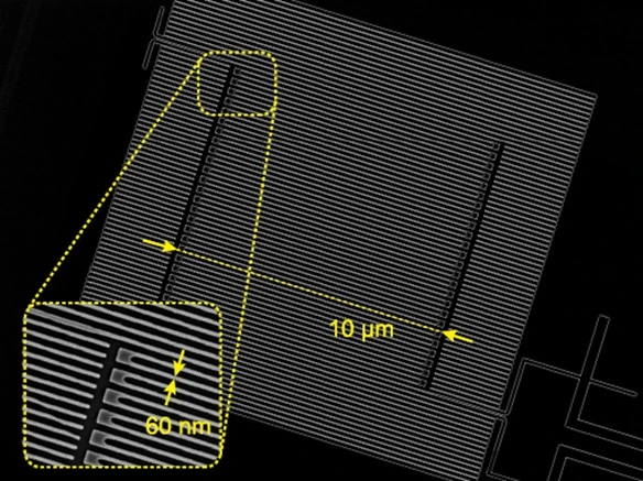
Sputter deposition technologies, such as magnetron sputtering and ion beam sputtering, were among the first approaches employed for depositing thin superconducting films, mostly because of the long tradition and the good understanding of these processes, as well as the relatively easy experimental setup. As a practical example, the following figure shows a scanning-electron micrograph (SEM) of a fabricated Superconducting Nanowire Single-Photon Detector (SNSPD) in which NbN has been deposited as the superconducting material via sputtering.
Sputtering Parameters for Superconducting Thin Films
Although the principles of the mentioned processes are well understood, depositing superconductors (especially HTS thin films) requires some modifications and considerations. Most of HTS compounds have complex crystal structures that demand precise stoichiometric control. For instance, YBCO thin film deposition often favors co-evaporation techniques such as co-sputtering to achieve the correct composition. As another example, when depositing YBCO via magnetron sputtering, the film properties are highly sensitive to nearly all process parameters, including deposition mode (RF or DC), substrate position (on-axis or off-axis), target alignment, gas composition and common process parameters such as power, substrate temperature, and gas pressure.
Choosing a Proper Sputtering System for Superconducting Thin Films: A Case Study
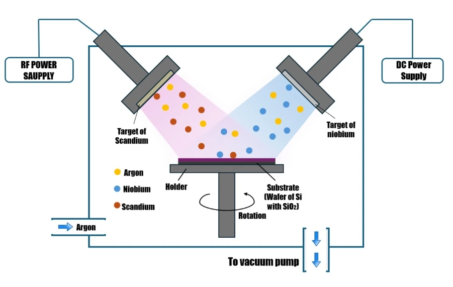
Since thin films superconductors are usually composite materials, co-deposition process are required to achieve the precise structures. So, co-sputtering by multi-cathode sputter coaters seem to fulfill the purpose, making DST3-A an ideal coating system for this application.
Among the various superconductive thin films, NbSc films have been deposited by DST3 Co-deposition of Nb and Sc targets to create Nb1-xScx through DC and RF co-sputtering, respectively.
References
- Bussmann-Holder, A., & Keller, H. (2019). High-temperature superconductors: Underlying physics and applications. Zeitschrift Fur Naturforschung - Section B Journal of Chemical Sciences, 3–14. https://doi.org/10.1515/znb-2019-0103
- Keysan, O. (2013). Application of high-temperature superconducting machines to direct drive renewable energy systems. Electrical Drives for Direct Drive Renewable Energy Systems (pp. 219–252). Elsevier Ltd. https://doi.org/10.1533/9780857097491.2.219
- Ersoz, T. T., Mohamed, A. E. M. A., & Attallah, M. M. (2025). Additive manufacturing of superconductors: Opportunities and challenges. Materials Research Bulletin (Vol. 189). Elsevier Ltd. https://doi.org/10.1016/j.materresbull.2025.113448
- Stoessel, C. H., Bunshah, R F, Prakash, S, & Fetterman, H. R. (1993). Thin-Film Processing of High-TC Superconductors. Journal of Superconductivity (Vol. 6, Issue 1). https://doi.org/https://doi.org/10.1007/BF00618500
- Deyu, G. K., Wenskat, M., Díaz-Palacio, I. G., Blick, R. H., Zierold, R., & Hillert, W. (2025). Recent advances in atomic layer deposition of superconducting thin films: a review. Materials Horizons (Vol. 12, Issue 15, pp. 5594–5626). Royal Society of Chemistry. https://doi.org/10.1039/d5mh00323g
- Colangelo, M., Walter, A. B., Korzh, B. A., Schmidt, E., Bumble, B., Lita, A. E., Beyer, A. D., Allmaras, J. P., Briggs, R. M., Kozorezov, A. G., Wollman, E. E., Shaw, M. D., & Berggren, K. K. (2022). Large-Area Superconducting Nanowire Single-Photon Detectors for Operation at Wavelengths up to 7.4 μm. Nano Letters, 22(14), 5667–5673. https://doi.org/10.1021/acs.nanolett.1c05012
- Kim, C. J. (2019). Superconductor Levitation: Concepts and Experiments. In Superconductor Levitation: Concepts and Experiments. Springer Singapore. https://doi.org/10.1007/978-981-13-6768-7
- Berezhnoy, P. A., et al. "Superconducting properties of Nb 0.85 Sc 0.15 film deposited by magnetron co-sputtering." Superconductor Science and Technology 39.8 (2026): 085033.