Surface Modification with Thin Films lithography
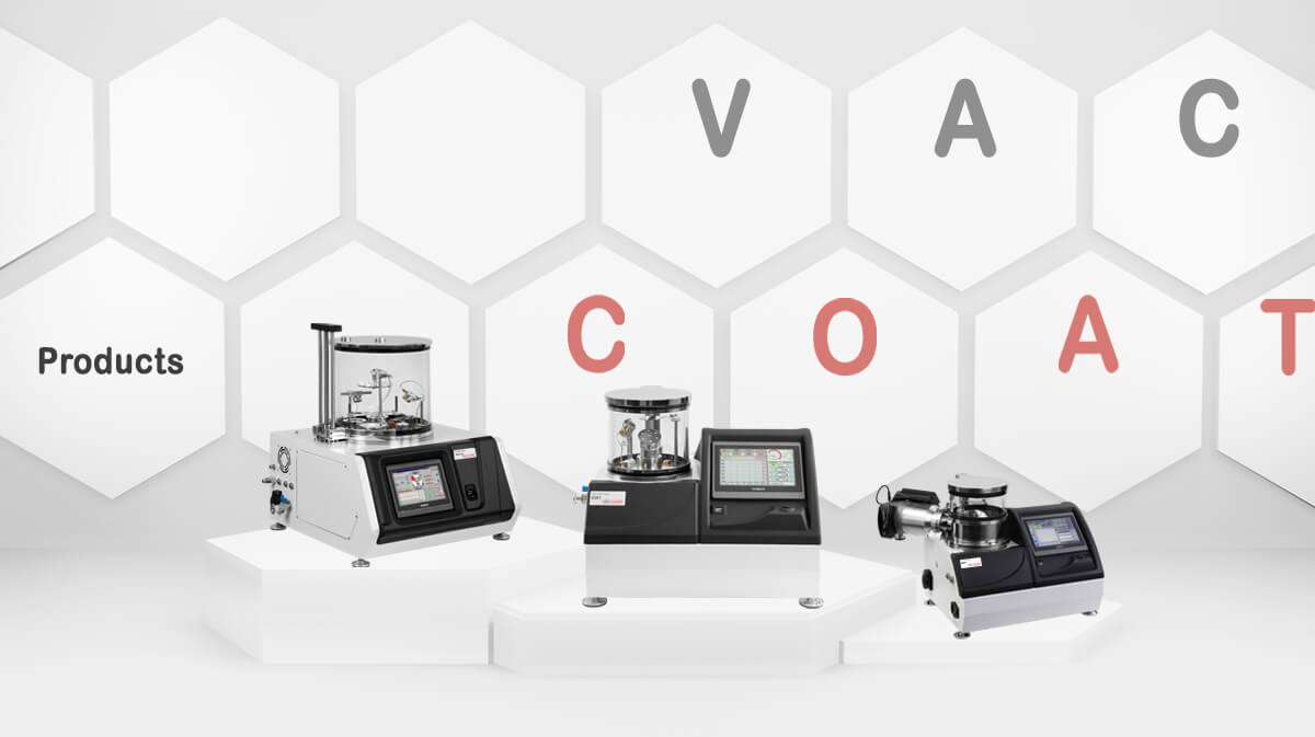
With the development of technology, microelectronics and microfabrication technologies were tasked with minimizing device components as much as possible. Therefore, scientists tried to find new methods of lithography. As a result, we focus on optical lithography, which is the most common type of it. Therefore, Vac Coat Company designs and manufactures three vacuum coating systems called DST3, DST3-T, and DTT, which provide cost-effective and advanced multifunctional thin films for lithography.


Since many physical and chemical properties of nanostructures are highly dependent on their surface, the surface modification in micro and nanometer scales has attracted a lot of attention. In addition, microsystems have been used in a wide range of industries such as biomedicine, mechanics, optics, fluid dynamics, MEMS microelectronics, and many more. Therefore, surface engineering has played an important role in the fabrication of micro and nano-sized systems. Surface modification methods include creating high-quality coatings using physical evaporation techniques as well as thin films lithography (optical and electron) methods.
On the other hand, the top-down fabrication method uses two main steps to fabricate microsystems:
-
- Create a thin film
- Create the desired patterns through optical lithography


Various coatings based on a variety of organic or mineral materials in nanometer-to-cm thicknesses can be created using top-down methods including physical vapor deposition (PVD) such as sputtering, carbon coating, pulsed laser deposition, thermal deposition, or chemical vapor deposition (CVD).
These layers are usually composed of thin films of metal, silicon, silicon dioxide, etc. Depending on the pattern, each layer requires a different mask for lithography. Therefore, the coating and the lithography processes may be repeated several times during the fabrication of a microsystem.
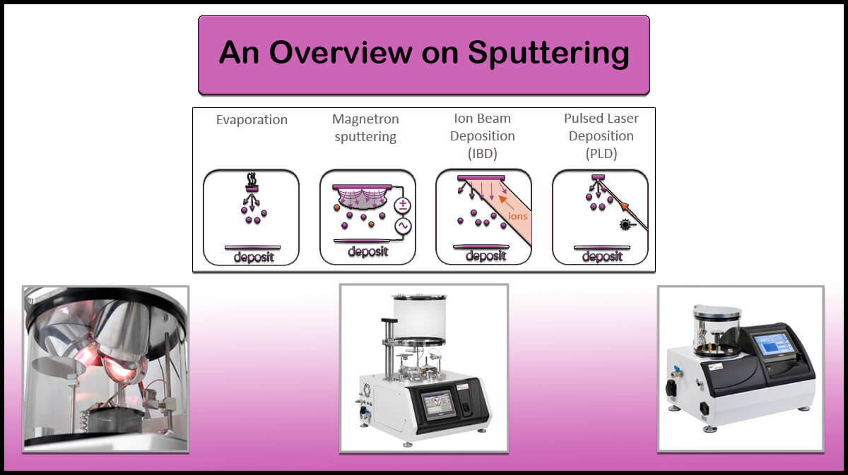

Physical Vapor Deposition (PVD)
Physical vapor deposition or PVD is a coating technique in vacuum condition for coating materials on an atomic scale in the form of thin films.
PVD can be described according to the following steps:
-
- Firstly, the material which should cover surfaces is evaporated by physical means
- Then the vapor is transferred through a low-pressure area and source to the desired surface
- After that, the vapor condenses on the surface to prepare a thin film


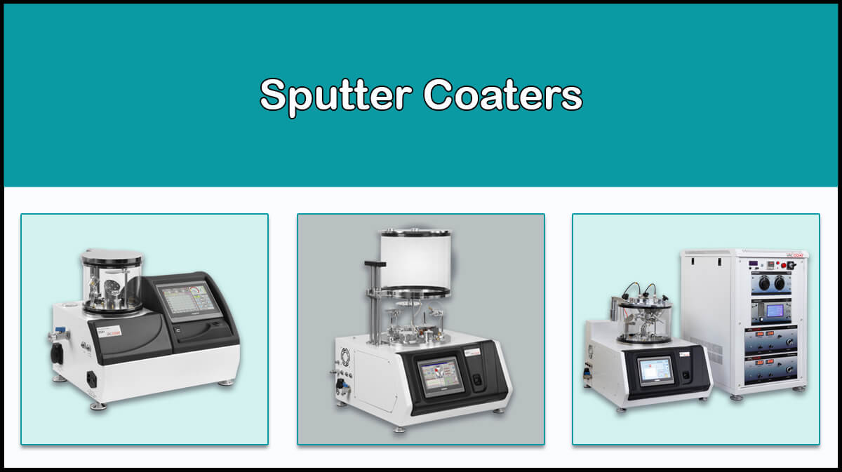
PVD processes are generally used to deposit films with thicknesses ranging from nanometers to centimeters. However, PVD can also be used to form multilayers and heterostructure coatings. The Vac Coat company recommends DST3-T, DST3, and DTT coaters for this range of vacuum coating processes to prepare the cost-effective and advanced multifunctional thin film for lithography.
The DST3-T is a triple target turbo pumped sputter coater that combines thermal evaporator and sputter coater in one single compact desktop system. The multi vacuum coater system is suitable for a wide range of materials deposition. The high vacuum coater can easily switch between evaporation and sputtering condition (Not Simultaneously).
The DST3 is a triple target sputter coater with water-cooled cathodes that can sputter semiconductors, dielectrics, and metal targets (More about Sputtering Targets). In addition, DST3 is equipped with an auto adjustable matching box and a large chamber.


Furthermore, DTT is a desk thermal evaporator equipped with a turbomolecular pump and triple source for thin films deposition. One of the DTT advantages is reaching the desired pressure in a short time and it is used in preparing SEM samples and thin films applications as a SEM Coater.


Lithography and Photolithography
Lithography is the creation of the desired pattern on the surface using shadow masks. The process was first invented by Alois Senefelder in 1796. Photolithography or optical lithography is the simplest method to create regular patterns in the nanometer or micrometer dimensions on the surface of a thin film or bulk material. In this method, the pattern of the shadow mask can be transferred on the layer using photoresists, which are light-sensitive polymers.

Optical lithography consists of three principal steps:
- Covering surface with radiation-sensitive polymer (Photoresist)
- The photoresist is exposed to UV radiation while covered with a photomask
- Remove photoresist by a suitable solution and then transfer the pattern on the surface by etching away the areas uncovered by the mask
Nowadays, it is used to create a pattern in the manufacturing of electronic components that scientists routinely use every day in laboratories. The main advantage of the technique is the production of patterned structures in micro and nanometer sizes with controllable geometry. Surfaces made through lithography can be used in a variety of fields such as biology, microfluidics, laboratory devices, chip fabrication, MEMS/NEMS, 3D microstructures, and nano-photonics.