What is Physical Vapor Deposition (PVD)?
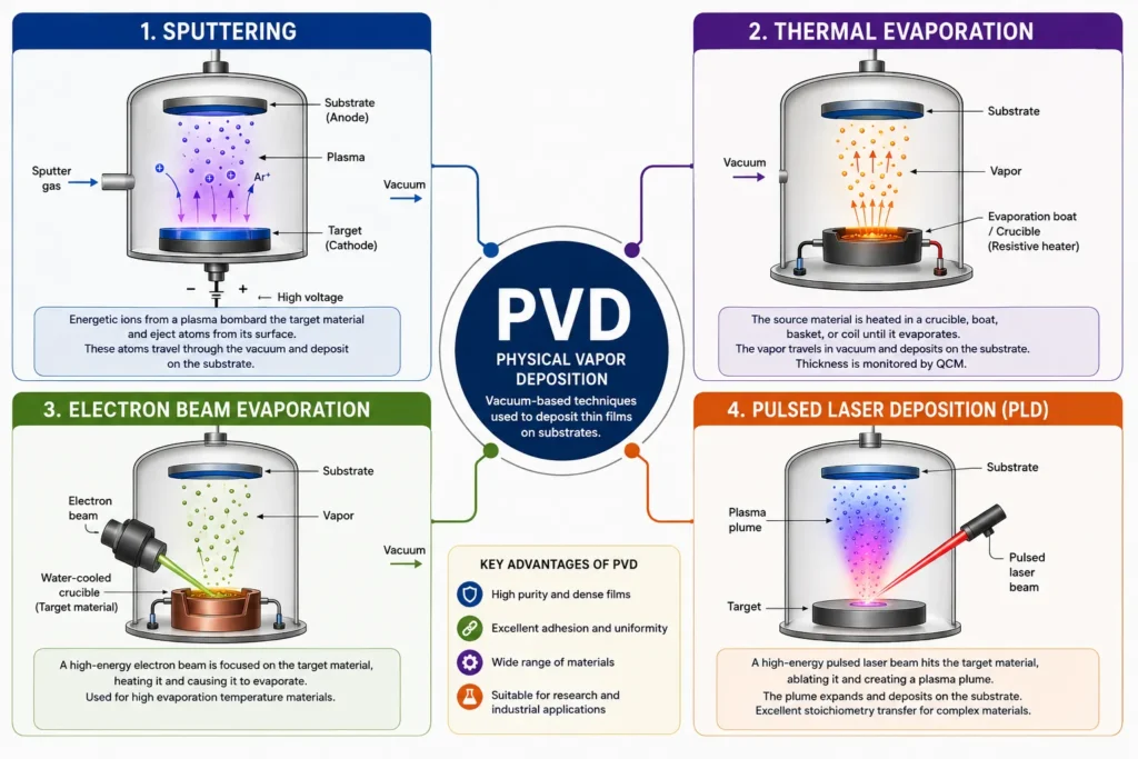
Physical Vapor Deposition or PVD is a group of vacuum deposition methods in which a solid material is vaporized in a vacuum environment and deposited as a thin film on a substrate. The most common PVD methods are sputtering and thermal evaporation.
In the PVD process, the desired material is transferred and deposited atom by atom or molecule by molecule onto the substrate surface in a vacuum environment, thus creating thin layers with controlled thickness, high purity, and specific physical, chemical, mechanical, or optical properties, making it superior compared to other deposition methods for many applications.
PVD technology is used in the production of semiconductor components, microelectronics, sensors, optical devices, solar cells, cutting tools, medical equipment, anti-wear coatings and many industrial products due to the possibility of precise control of the thickness, composition, structure and properties of the thin layer.
How is the physical vapor deposition process?
In a PVD deposition system, first the chamber is evacuated to a pressure of at least 10-4 Torr to reduce unwanted gases and impurities inside the coating chamber and increase the mean free path, which is the average distance between collisions of gaseous particles. Then, the desired substance, which is called the target or evaporation source, is converted into the vapor phase by one of the appropriate methods and reaches the surface of the sample almost in a straight line, with few collisions with the remaining gas particles inside the chamber.
Some common PVD technologies for transferring the target material to the vapor phase are:
- Sputtering
- Thermal Evaporation
- E-beam Evaporation
- Pulsed Laser Deposition
The selection of the appropriate method depends on the material type, desired thickness, substrate type, process temperature, deposition rate, and required layer properties.
Types of Physical Evaporation Deposition Methods
PVD technology is a set of different techniques that have been developed for different applications. The most important methods are:
Sputtering method
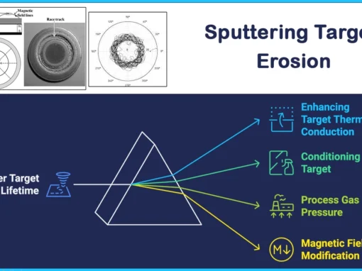
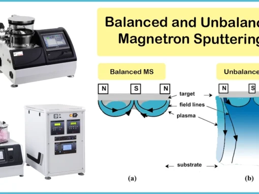
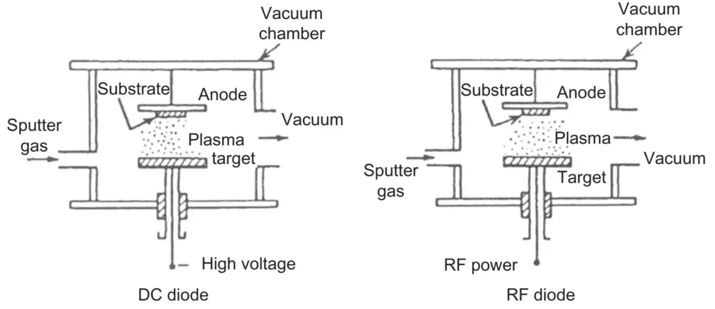
Sputtering is one of the simplest and most widely used deposition methods for various materials. In sputtering, a high-voltage power supply is used to create a plasma of energetic ions, usually argon ions, which bombard the target material and separate the atoms of the material from its surface. These atoms move in a vacuum and are deposited on the substrate.
This method is used to produce thin films of various materials from metals such as gold, silver, platinum, copper, aluminum in direct current sputtering (DC sputtering) and non-conductive or dielectric materials using alternating current sputtering (RF sputtering).
The sputtering method has various types, such as magnetron sputtering (with a magnetic cathode), pulsed sputtering, and reactive sputtering, depending on the type of cathode and power source for producing the plasma and other deposition conditions. High-Power Impulse Magnetron Sputtering (HiPIMS) is an advanced generation of sputtering that uses very high power in the form of short pulses to increase the density of plasma and target ions, allowing the production of coatings with desirable density, adhesion, and mechanical properties.
Thermal Evaporation; the most common PVD method
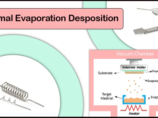
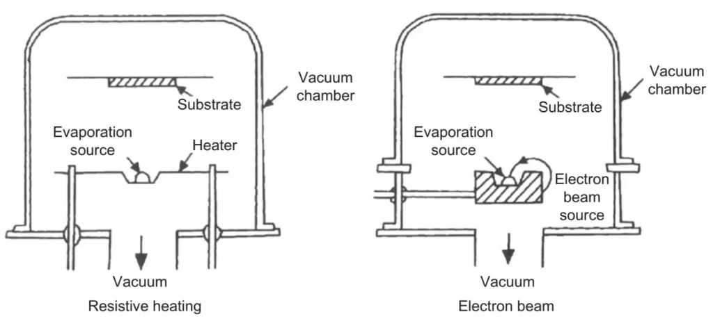
Thermal evaporation is one of the oldest and most widely used physical vapor deposition methods. In this technique, the source material is placed inside a resistive heat source such as a crucible or evaporation boat, basket, or coil, and heated by passing an electric current.
This method is used to evaporate materials with relatively low melting temperatures such as gold, silver, aluminum, copper, nickel and other metals, and is used in academic research, manufacturing electronic devices, optics, sensors and the production of laboratory thin films.
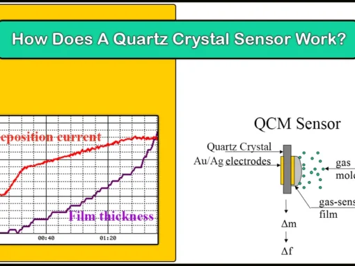
In advanced PVD systems, the use of Quartz Crystal Microbalance or QCM allows for the instantaneous measurement and control of the growth rate and thickness of the layer.
Electron Beam Evaporation
In this method, a high-energy electron beam is focused on the target material in a crucible in a vacuum chamber, raising its temperature and causing it to evaporate. This method is mostly used for the deposition of materials with high evaporation temperatures.
Pulsed Laser Deposition
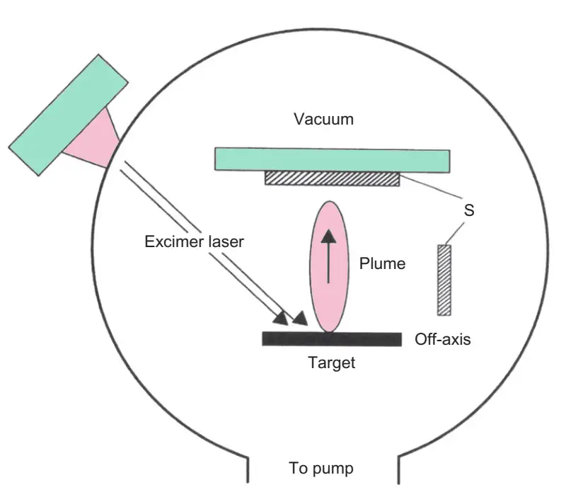
In the PLD method, a plasma plume is created by a high-energy laser beam radiation on the target material, which extends to the substrate and is deposited on it. Due to the high power of the laser, the atoms of the composite targets are transferred to the substrate with enhanced stoichiometry conservation compared to other physical vapor deposition methods.
Applications of Physical Vapor Deposition
Today, PVD is considered as one of the key technologies in the development of advanced materials and manufacturing of modern devices.
1. Semiconductors and Microelectronics
In the semiconductor industry, precise control of layer thickness and composition is of great importance. PVD is used to create metal layers, barrier layers, electrodes and multilayer structures vital in microelectronic devices.
As the dimensions of electronic components have become smaller, the need for thinner, more uniform and cleaner films has also increased.
2. Solar cells and renewable energies
Thin layers play an important role in various solar cell technologies. PVD methods are used to produce metal layers, conductive layers, reflective layers, as well as functional materials, useful in green-energy technologies.
In this area, controlling the thickness and optical properties of the layer can directly affect the final performance of the component.
3. Optics and Photonics
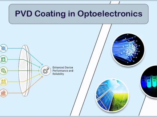
One of the important applications of PVD is the production of optical coatings. By designing the thickness and refractive index of the layers, coatings can be produced to increase or decrease reflection, control light transmission, and create special optical properties.
Multilayer PVD coatings are used in lenses, optical filters, laser equipment, detectors, and other photonic systems.
4. Cutting tools and hard coatings
The atom-by-atom deposition by PVD methods allows control of the density, stoichiometry, and atomic structure of thin film coatings. Using the right materials and creating specific conditions during the deposition process, can lead to creation of coatings with desirable properties such as hardness, softness, and proper adhesion on various surfaces. One of the best-known applications of PVD is the production of hard coatings for cutting tools. Coatings such as TiN, TiAlN, and more advanced compounds can increase surface resistance to wear and high temperatures. For example, titanium nitride coatings have high resistance to wear and corrosion, along with the attractive shinny view, are used to coat building valves and door handles that are constantly in contact with the hand.
This technology is used in turning tools, milling tools, molds, drills, and parts that are subjected to friction and mechanical load, such as defense industries, cutting tools, rollers, and many other cases where reducing friction is of great importance.
5. Medical equipment and biomaterials
In medical equipment, surface engineering can change the surface characteristics without significantly changing the properties of the base material. PVD has been considered for producing some wear and corrosion-resistant coatings and modifying the surface characteristics of parts of medical equipment.
6. Automotive and aerospace industries
Reducing friction, increasing wear resistance, and improving the durability of parts are important coating goals in the automotive and aerospace industries. PVD coatings can be used on mechanical parts, tools, engine components, and surfaces that are exposed to harsh working conditions.
PVD Coating and Nature
The physical vapor deposition method involves environmentally friendly processes and, compared to other coating methods such as chemical plating, greatly reduces the use of toxic raw materials, chemical reactions, and disposal of chemicals resulting from the reactions.
Advantages and disadvantages of PVD coating
The following are some of the advantages of physical vapor deposition coating:
- Creating very thin and uniform layers
- Precise control of thickness and deposition rate
- High purity of the film under appropriate process conditions
- Enabling controlling the structure and composition of the layer
- Ability to produce resistant coatings against wear, corrosion and high temperatures
- Possibility of coating a wide range of organic and inorganic materials on various surfaces
- Possibility of producing multilayer and nanostructured coatings
- Cost-effectiveness with reduction of material consumption compared to using bulk material
- Wide range of process parameters enables achieving desired film structures
- Widespread use in research and development and industrial production
- High environmental compatibility
Limitations of PVD
Despite its many advantages, PVD also has limitations. Many processes require a suitable vacuum system, precise control equipment and a skilled operator. Also, in some methods, the deposition occurs in straight a line-of-sight between the source and the substrate, which makes it more difficult to coat porous or uneven surfaces.
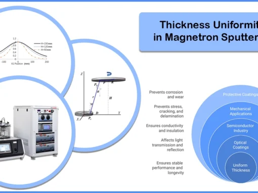
However, these issues can be solved by the use of substrate rotation, planetary motion, substrate bias (bias sputtering), multiple deposition sources, and appropriate plasma field design, which can greatly improve the uniformity and coverage of complex surfaces.
Also, some PVD methods and techniques require high user attention and precision due to the vacuum and high temperature of the deposition environment, and require water-cooling systems to dissipate the heat generated and prevent damage to the components of the deposition systems.
The Future of Physical Vapor Deposition Technology
The development trend of PVD is moving towards more precise process control, reduced energy consumption, multilayer and nanostructured coatings, better control of ions and plasma, and automation of the deposition process.
By precisely controlling the deposition process, structures with very thin thicknesses can be created, with each layer having a different function. These structures allow for the combination of features such as improved hardness, excessive adhesion, corrosion resistance, optical properties, and electrical conductivity.
For this reason, modern PVD devices usually provide the researchers with the ability to precisely control pressure, deposition power, process gas, substrate movement, deposition rate, and layer thickness.
With the development of semiconductors, renewable energy, photonics, sensors, medical devices and advanced materials, the demand for deposition systems with precise controllability will increase. For this reason, sputtering machines, thermal evaporation systems, magnetron sputtering devices, research PVD systems and multi-purpose deposition systems have become important tools in R&D laboratories and advanced production lines.
How to choose the right PVD coating system?
The selection of a PVD deposition machine should be based on the desired application. Parameters such as the target material, desired film thickness, sample size, and coating uniformity should be determined before purchasing or designing a system.
Also, the required technique to evaporate the target material, the power source properties, the number of cathodes (in sputtering process), the size of the vacuum chamber, the vacuum pump capabilities, the base pressure, the gas control (if required), the substrate stage features (including rotation system, substrate heating or biasing), and the thickness measurement system should also be considered.
The system flexibility is particularly important for research applications, since the researcher may use different deposition techniques and materials for various research projects.
Summary
Physical vapor deposition (PVD) is an important technology for thin film production and surface engineering, which allows for control of material properties on a very small scale. From producing hard coatings on cutting tools to creating functional layers in semiconductors, solar cells, optical devices, sensors, and medical devices, PVD plays a critical role in today’s technologies.
The correct choice of deposition method, target or evaporation source, vacuum conditions, process gas, power, substrate temperature, and thickness control system determines the quality of the final film. For this reason, a suitable PVD system is not just a vacuum chamber and deposition source; it is an integrated set of vacuum system, vapor generation source, gas control, substrate holder features, and process monitoring tools.
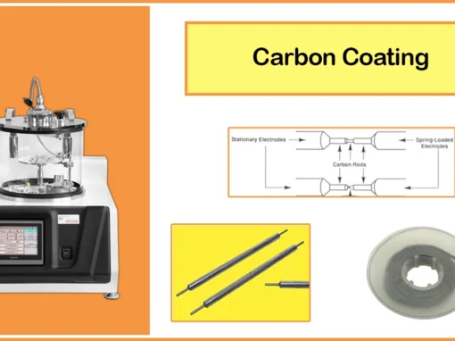
Vac Coat deposition systems, using physical vapor deposition techniques, enable users to deposit a wide range of materials onto various substrates, depending on their desired performance. The ability to use two PVD techniques in one coating machine has eliminated the problems of purchasing different machines for coating different materials. Vac Coat combined coating systems are offered in various models, including DST3-T model with top-down sputtering, along with thermal evaporation, as well as bottom-up sputtering and thermal evaporation in glovebox compatible DST2-TG, and models DSCR and DSCT that combine sputter coating and carbon (fiber threads or rods) evaporation.
References
[1] Mattox, D. M. (2010). Handbook of Physical Vapor Deposition (PVD) Processing (2nd ed.). William Andrew/Elsevier.
[2] Ohring, M. — Materials Science of Thin Films: Deposition and Structure, 2nd ed., Academic Press. Broader thin-film science text; strong on nucleation/growth theory and structure-property relationships.
[3] Gudmundsson, J. T., Anders, A., & Von Keudell, A. (2022). Foundations of physical vapor deposition with plasma assistance. Plasma sources science and technology, 31(8), 083001.
[4] Rossnagel, S. M. (2003). Thin film deposition with physical vapor deposition and related technologies. Journal of Vacuum Science & Technology A: Vacuum, Surfaces, and Films, 21(5), S74-S87.
[5] Physical Vapor Deposition of Thin Films, edited by J. E. Mahan (Wiley, New York, 2000), p. 115.
[6] Adachi, Hideaki, and Kiyotaka Wasa. "Thin films and nanomaterials." Handbook of sputtering technology. William Andrew Publishing, 2012. 3-39.