Thickness Uniformity of Thin Film Deposition by Magnetron Sputtering
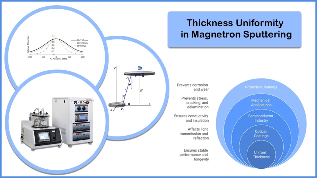
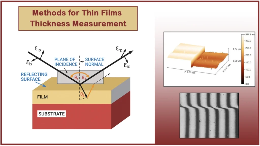
Thickness uniformity of thin films is an important feature in a coating performance that can be manipulated through adjusting deposition chamber geometrical factors.
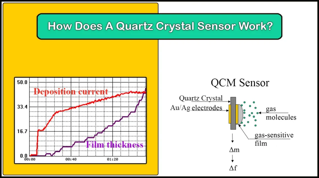
A quartz crystal microbalance (QCM) sensor is a piezoelectric crystal that detects the extra mass placed on it based on the change in its resonating frequency.
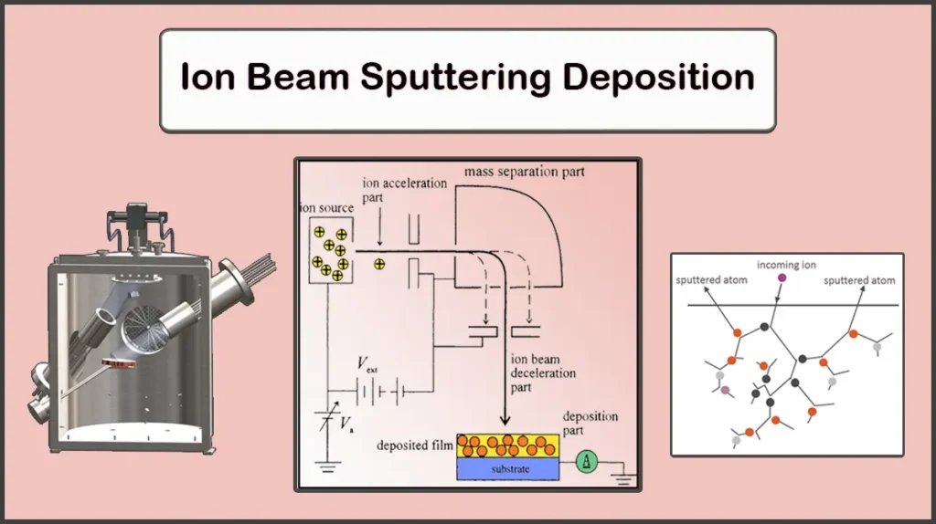
Ion Beam Sputtering Deposition is one of the favorable methods to form high purity, uniform, and dense thin films resulting from energetic ion sputtering of the target material.
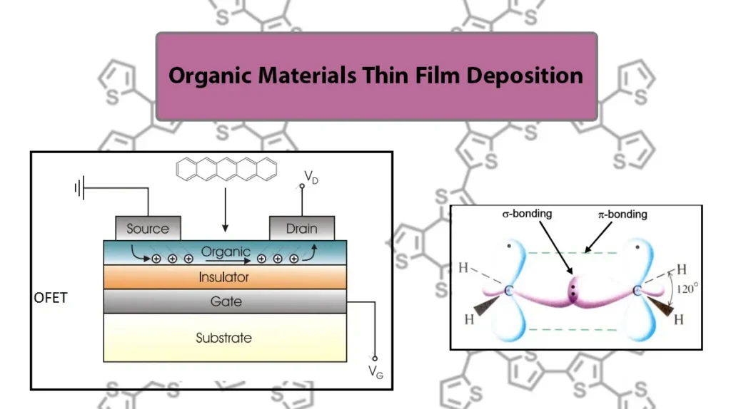
Organic materials play an important role in development of electronic and electro-optic devices due to their electronic band structure, low cost, and high flexibility.
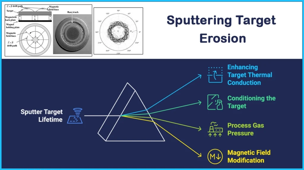
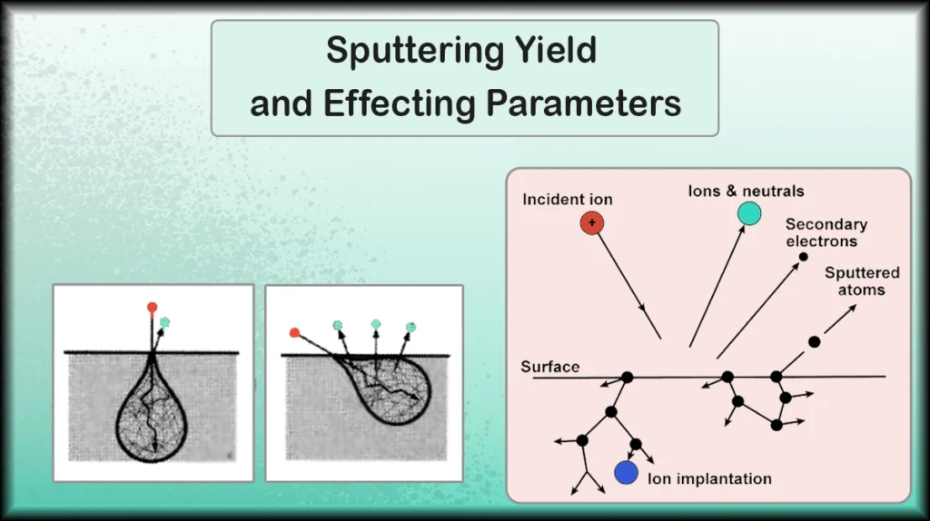
Sputter yield is a key parameter in the sputter coating process that highly affects the sputtering efficiency and the deposition rate and is a function of several factors, including energy and target material.
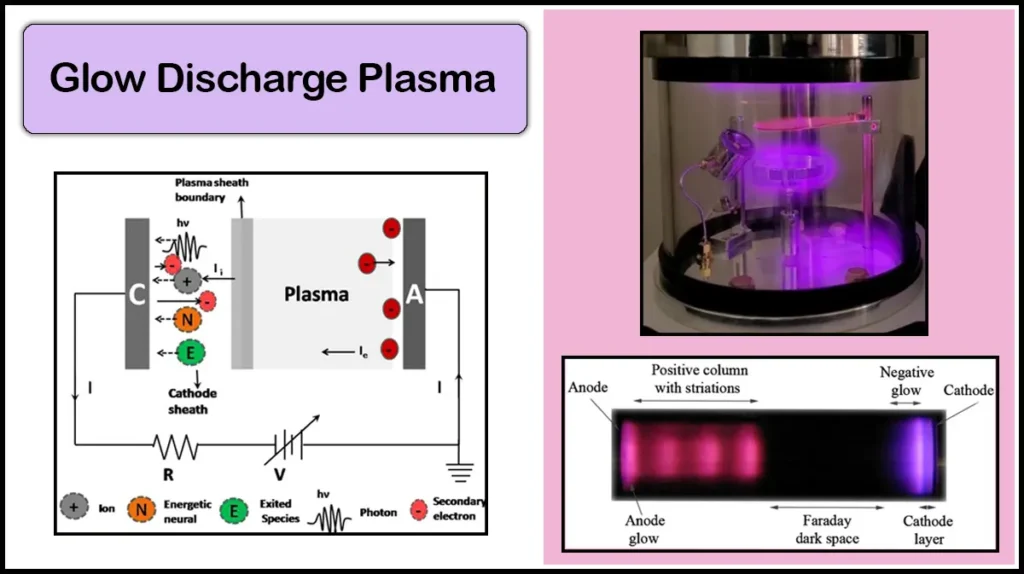
Glow Discharge Plasma is a colored plasma generated by passing electrical current through an ionized gas between two electrodes with many application, from light bulbs to sputter coating.
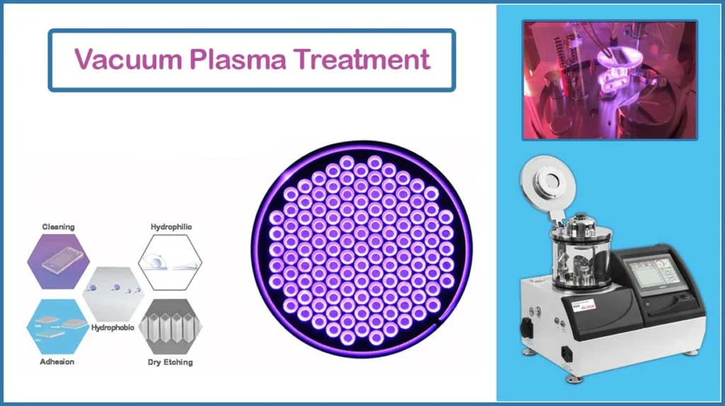
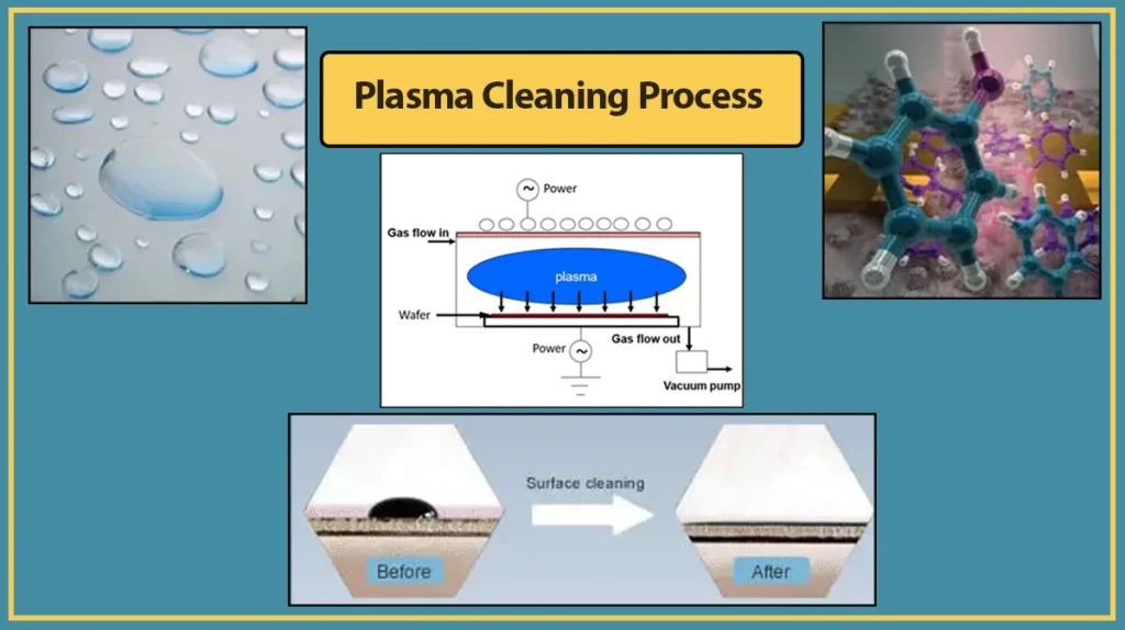
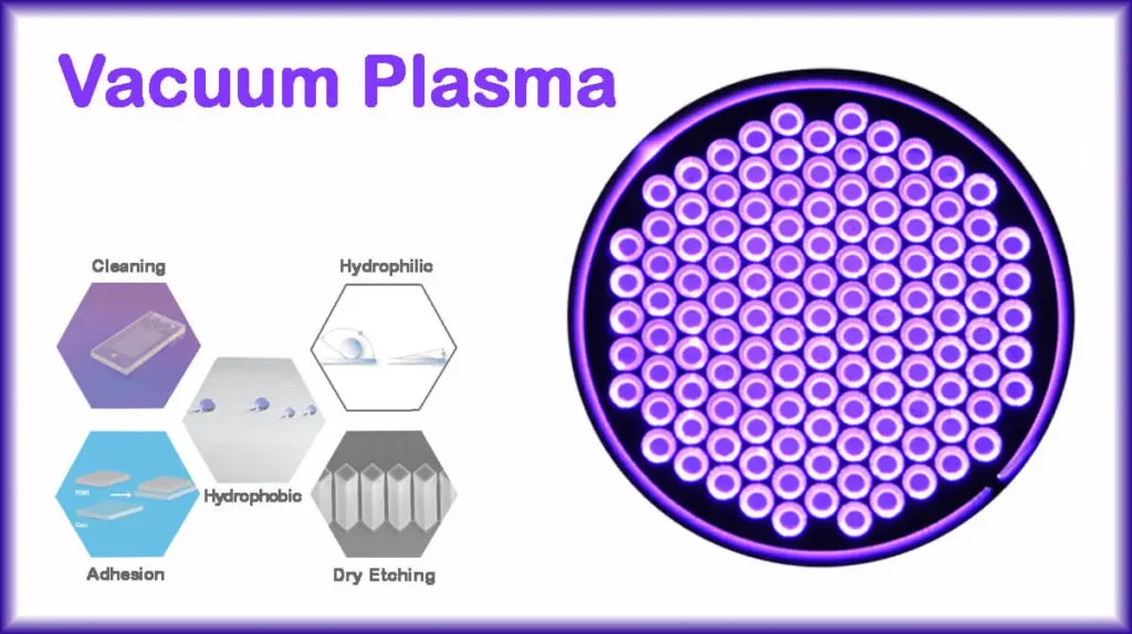
Plasma cleaning is an efficient, eco-friendly, and versatile surface plasma treatment that facilitates cleaning a surface to the atomic level or create desired functional groups on it for different applications.
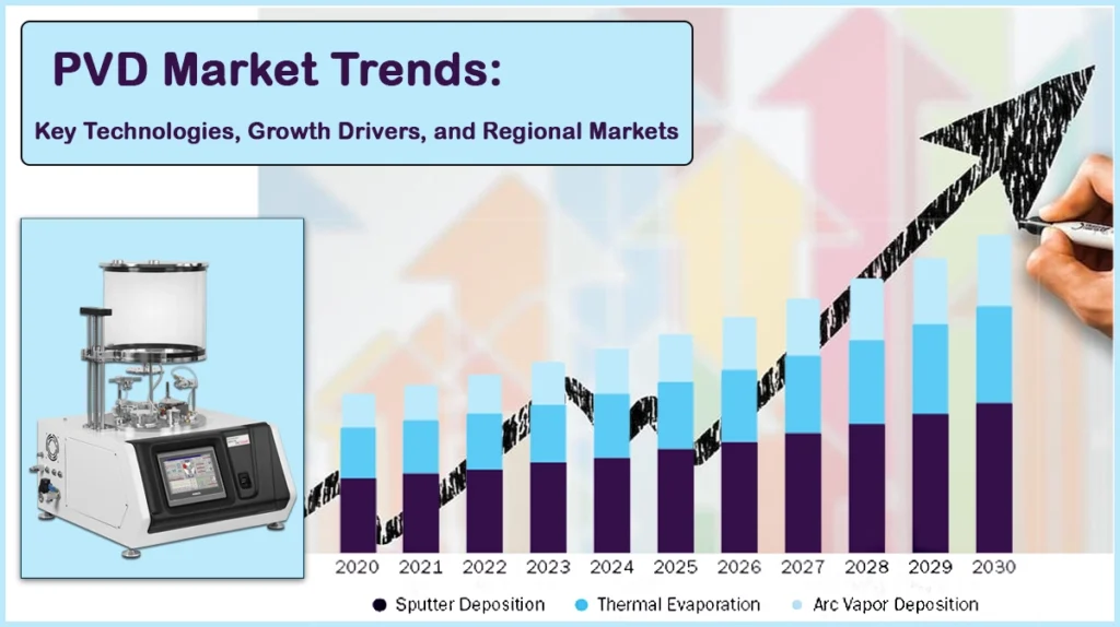
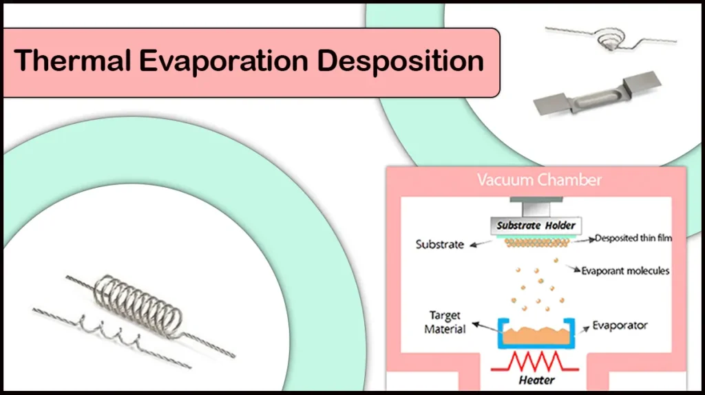
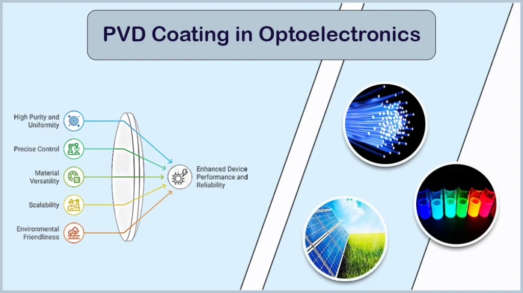
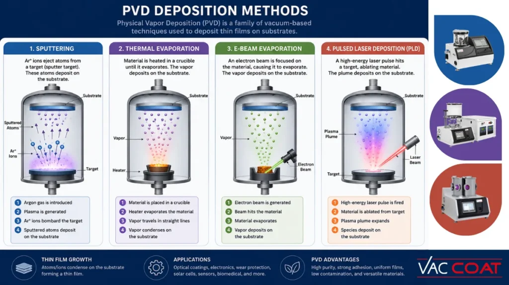
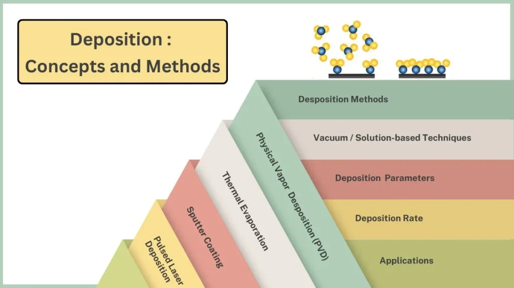
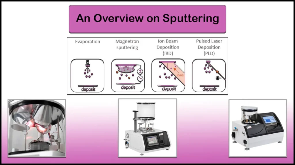
Physical Vapor Deposition (PVD) is a set of vacuum deposition methods in which a solid material vaporizes in a vacuum environment and is deposit on the substrate as a thin film.
Deposition on a surface based on different physical and chemical coating processes can modify its surface structure and properties that can lead to various applications.
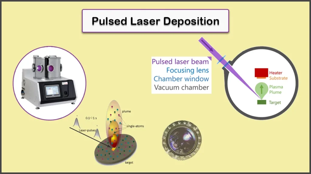
Pulsed Laser Deposition (PLD) is a high vacuum PVD technique in which a high-energy laser is used to ablate the target material and create a plasma plum with species of the same stoichiometry of the target to be deposited on the substrate.
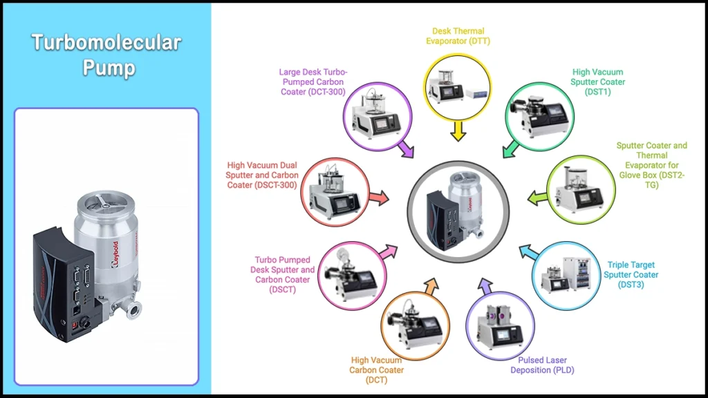
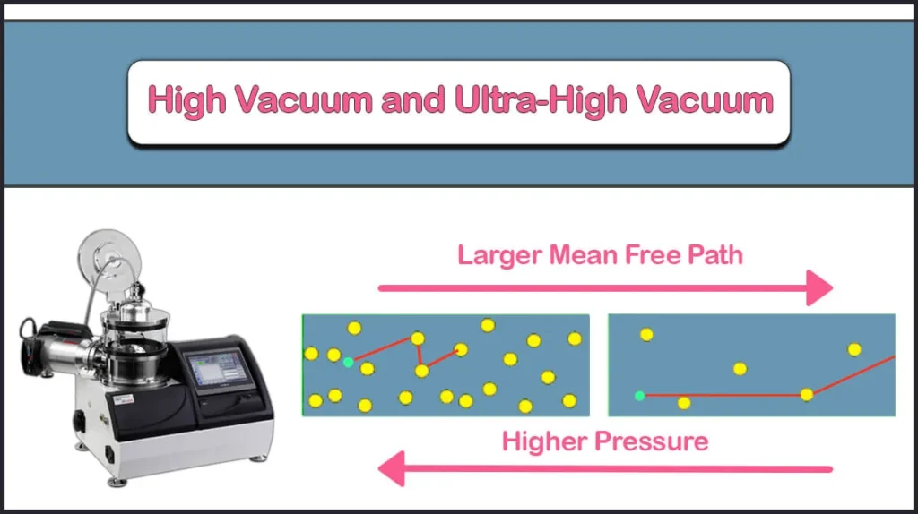
High vacuum and Ultra-high vacuum systems provide a clean environment for processes that needs clean surfaces, as thin film deposition and surface analysis.
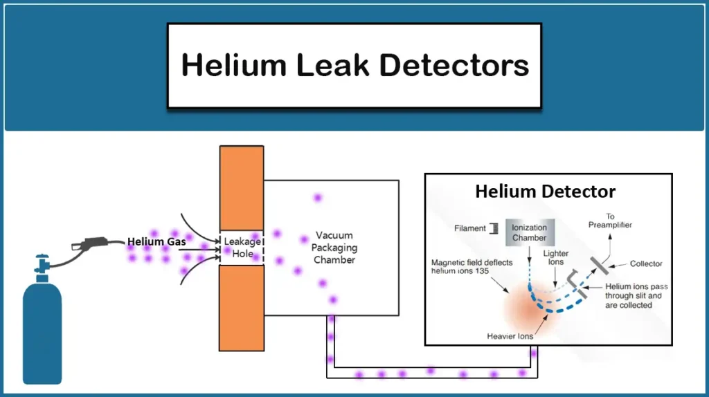
Helium leak detectors are high-precision vacuum leak detection systems used in finding local or integral vacuum leaks using various techniques like sniffer probe, spraying, etc.
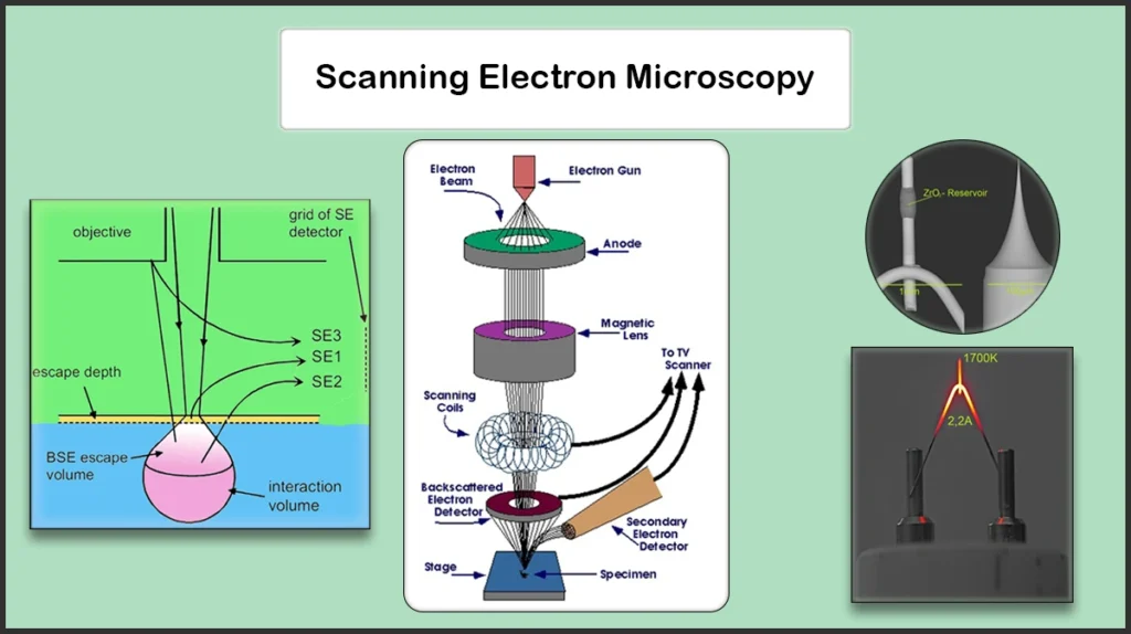
Scanning electron microscopy (SEM) is a highly efficient method for imaging micro-nano structures. SEM has improved enormously to enhance image quality.
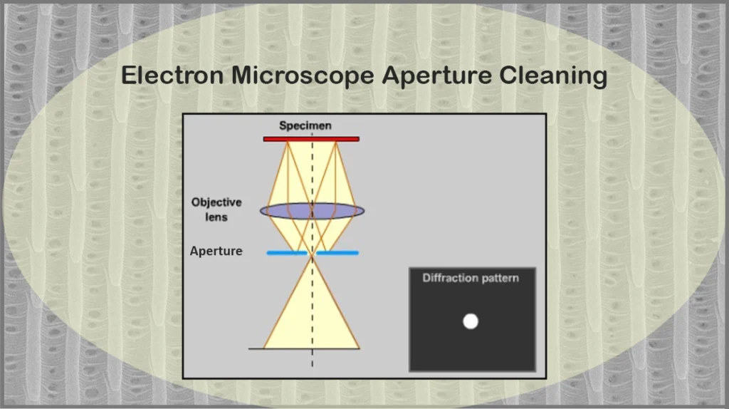
Aperture cleaning electron microscope is mainly achieved through thermal evaporation or plasma cleaning is an essential process to obtain high-resolution SEM/TEM images.
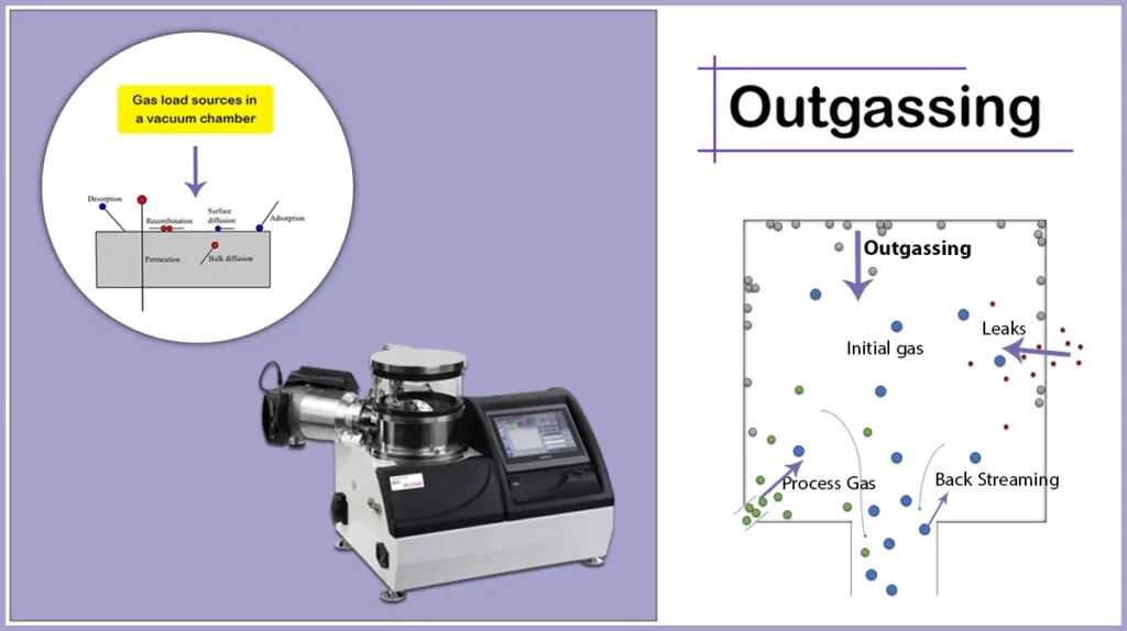
Outgassing is defined as the release of a gas which has been trapped, dissolved, absorbed or frozen in a material, a challenge in the way of high vacuum deposition.
Chalcogenide Thin Films Deposition | A Complete Overview
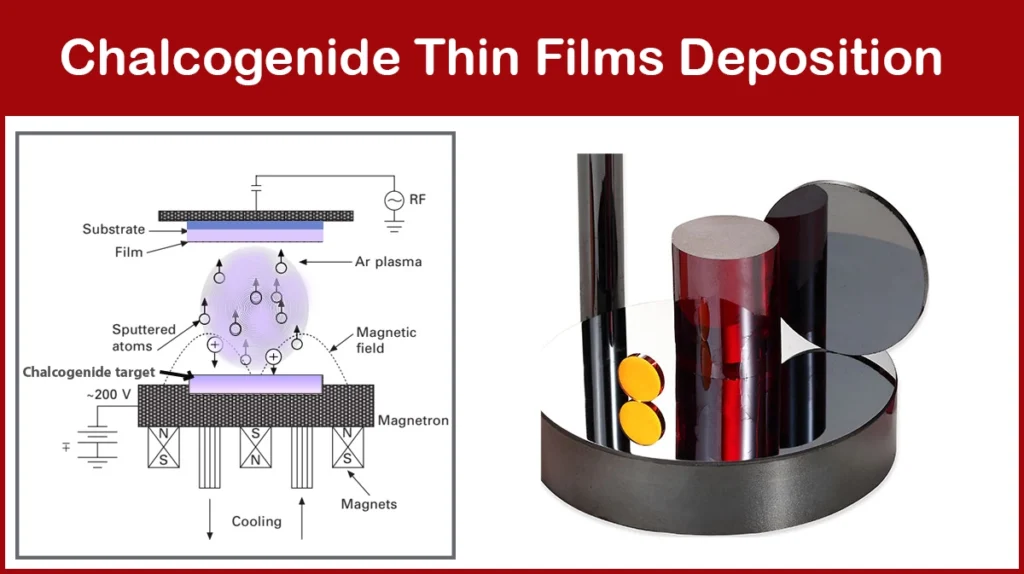
Chalcogenide thin films deposition through different coating methods such as sputtering, possess special properties for solar cells, fuel cell, batteries, etc.
Field Emission Scanning Electron Microscopy (FE-SEM)
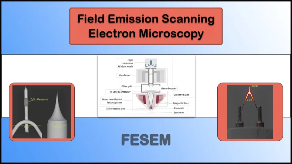
Field Emission Scanning Electron Microscopy (FESEM) is an improved version of SEM method with higher resolution imaging capability of micro and nano structures.
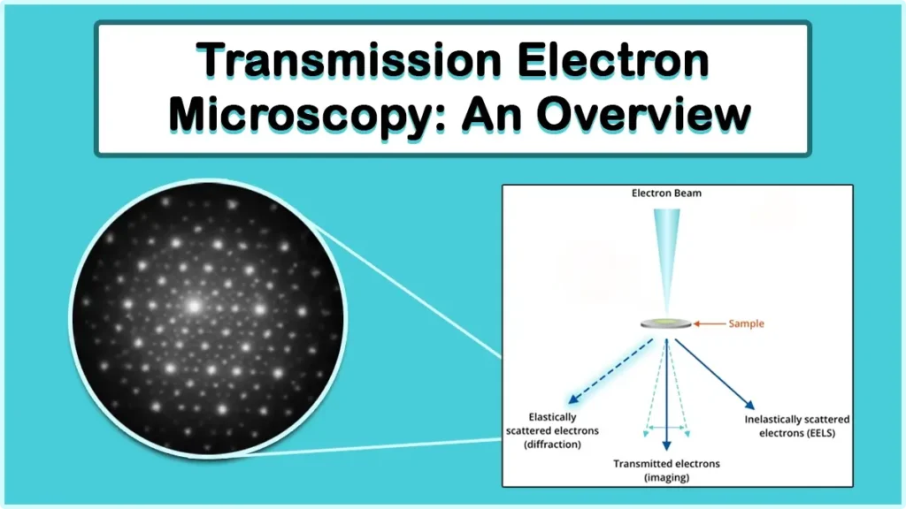
Transmission Electron Microscopy is a powerful tool that shows tiny structures in detail, allowing analysis of shape and elements of biological materials.
Electron Microscope Invention: A Historical Overview
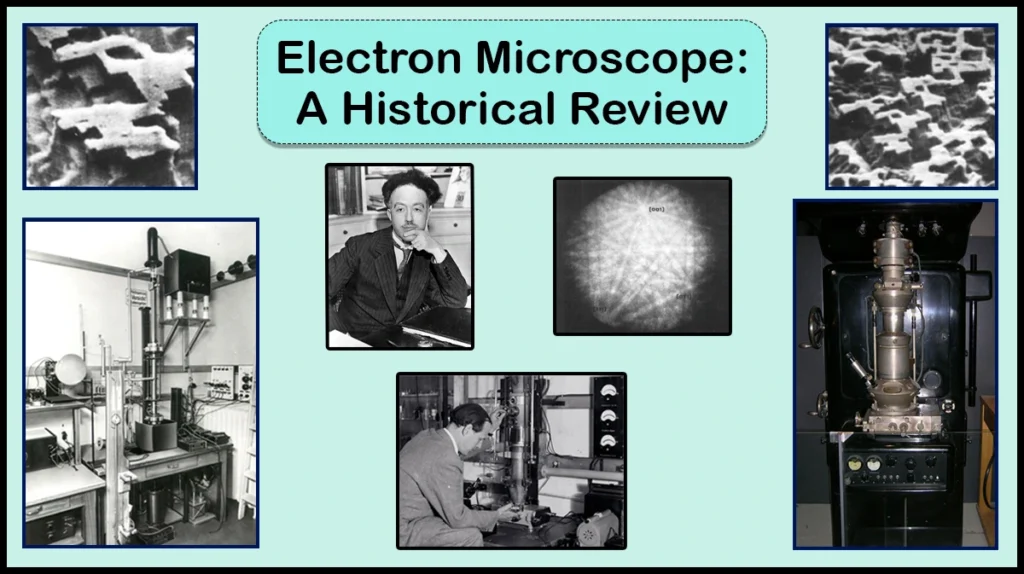
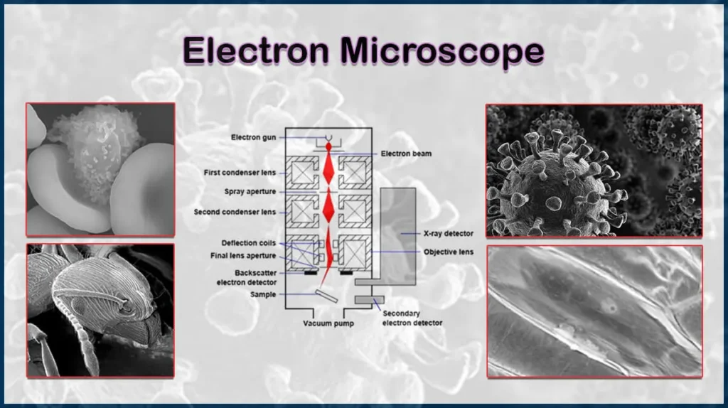
The history of electron microscope began in 1931 by Ernst Ruska and Max Knoll.Electron microscope invention created a powerful method for surface investigation.
Plasma is the fourth state of matter that can be reached in high energies. When atoms in a gas gain extremely high temperatures it goes to plasma phase.
Sample Preparation for Scanning Electron Microscopy
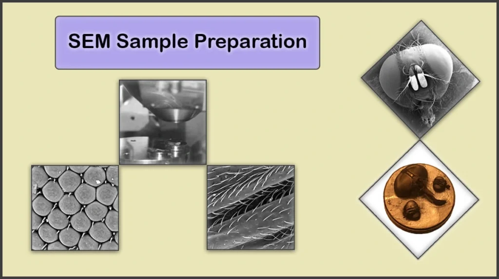
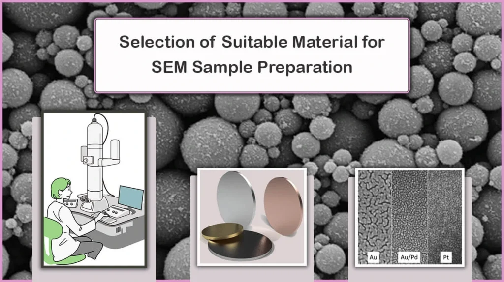
SEM samples need to be prepared by a sample preparation process to intensify image clarity and a clean, dried, and conductive sample is ideal for SEM imaging.
What is Energy-Dispersive X-Ray Spectroscopy (EDX)?
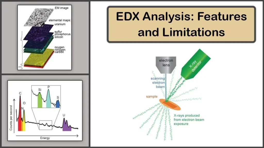
EDX is a tool for elemental analysis performed during EM through inelastic scattering of electrons with specimens and generation of X-ray characteristic peaks.
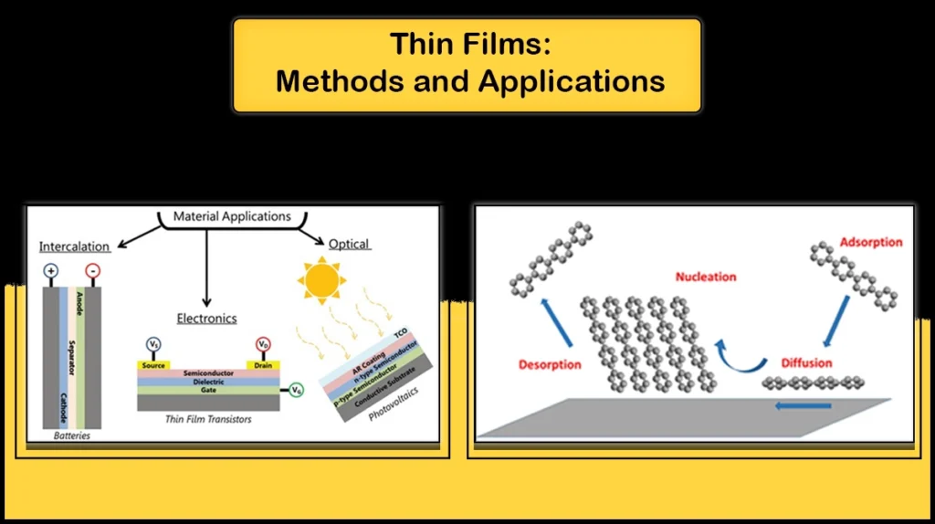
Thin film, deposition of a nano/micrometer thin layer, on the bulk material can help to improve its surface features, which is widely used in science & industry.
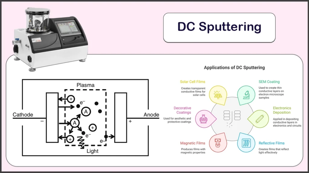
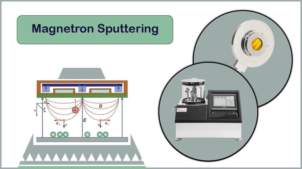
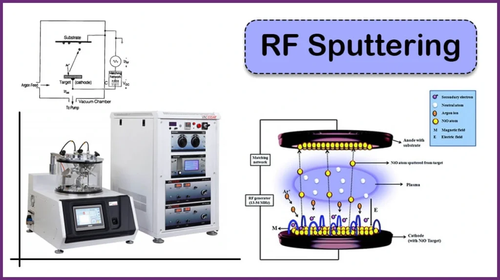
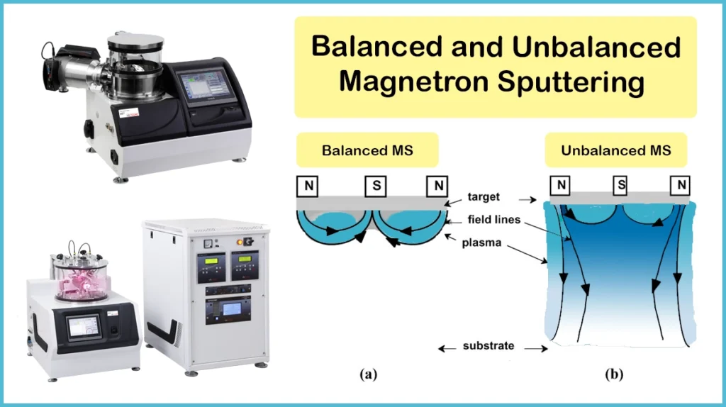
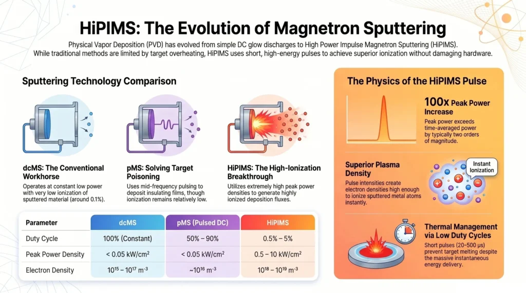
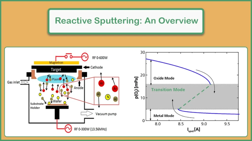
Sputtering is widely used in thin film deposition as a coating method and has developed extensively to achieve required properties for different applications.