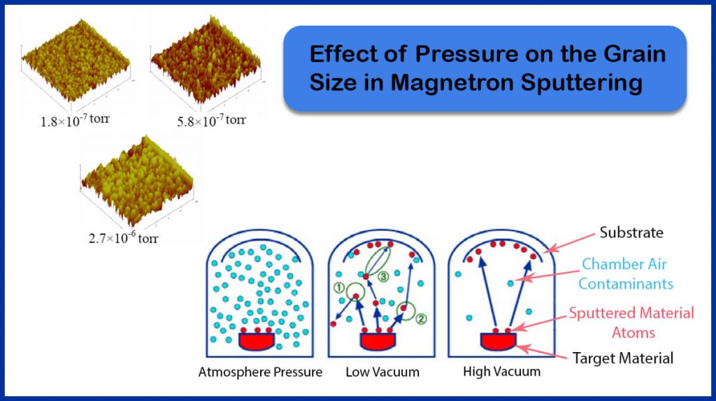
Effect of Base Pressure on Thin Film Grain Size in Sputtering
Sputter coating of thin films is operated in a vacuum chamber, where pressure is much lower than atmosphere environment, to reduce the air contaminants in the chamber and have a cleaner thin film. Pure argon purge into the chamber also helps to remove residual air and increase sputtering deposition rate. As the chamber is evacuated before argon purge, various contaminants of the environment like nitrogen, oxygen, carbon dioxide, and water vapor get out of the chamber gradually, where water vapor is the greatest barrier toward reaching higher vacuum levels.
Vacuum Pumps
Mainly two types of vacuum pumps are utilized, which result in different accessible vacuum levels. Medium vacuum level can be obtained by a rotary pump, whereas a turbomolecular pump backed with rotary pump is used to reach higher vacuum environments. For deposition of different materials with diverse applications different vacuum levels are needed.
Medium vacuum is sufficient for coating noble metals like Au and Au/Pd films, but it does not work for thin films of materials with finer grain size, like Chromium, Tungsten, and Iridium. Gold as a common conductive coating is mainly used for its high electrical conductivity, but its large grain size is not suitable to achieve high resolution thin films. Nowadays, metals like platinum, chromium or iridium are used in order to gain higher resolution coatings, but they require the use of turbomolecular pump to reach high vacuum in a conventional sputtering system [1,2].
Grain sizes of thin films of different materials (For different materials see Deposition Material Table) at needed vacuum levels for the purpose of sample preparation for scanning electron microscopy are listed below in Table 1.
As an example, for Pt coating, the presence of oxygen in the chamber environment results in cracks called “stress cracking”, indicating the important role of using a high vacuum sputtering system to gain a higher quality Pt thin film [1].
Also in another research investigating the effect of chamber pressure on platinum grains, it is shown that grains deposited at 100 mTorr appear more rounded as a result of collisions between the gas and sputtered metal atoms during deposition. Well-ordered nucleation sites at lower pressures result in a uniform surface morphology. At high pressures, these sites appear to spread out, and the grains appear smaller at lower pressures as observed in the plan view in Fig. 1 [3].
Sputter Coaters
Vac coat Ltd. products, include sputtering systems, carbon coating systems, thermal evaporation systems, and pulsed laser deposition systems, offer vacuum coating systems with rotary and turbomolecular vacuum pumps to provide different vacuum levels for high-quality thin film deposition.
Vac coat sputter coaters, DSR1 and DST1, use sputtering deposition method to make thin films. Desk Sputter Coater – DSR1 has a rotary pump and be able sputtering in lower vacuum but DST1 is equiped by a turbomolecular pump and works in higher vacuum conditions. Therefore, DSR1 and DST1 are two good choices of SEM Coaters to preparing samples for electron microscopes.
Triple Target Sputter Coater with a thermal evaporator (DST3 & DST3-T), magnetron desk sputter coater (DST1-300 & DST1-170), and turbo pumped desk sputter and carbon coater (DSCT & DSCT-T), are other Vac coat deposition systems working in medium and high vacuum conditions. For more information, visit the website please.
Related Posts
References
- https://www.cambridge.org/core/journals/microscopy-today/article/target-material-selection-for-sputter-coating-of-sem-samples/089A8657A8345CFFCF963BED868578D4
- https://www.emsdiasum.com/microscopy/technical/datasheet/sputter_coating.aspx
- “Effect of pressure on dc planar magnetron sputtering of platinum”, May 2003 Journal of Vacuum Science & Technology A Vacuum Surfaces and Films 21(3):572-576
- https://www.shinmaywa.co.jp/vac/english/vacuum/vacuum_2.html
- “Base Pressure Effects on the Structure, Surface Roughness and Electrical Resistivity of Mo Thin Films by RF Magnetron Sputtering”, February 2011 Advanced Materials Research, https://doi.org/10.4028/www.scientific.net/AMR.213.161

