What is Field Emission Scanning Electron Microscope (FE-SEM)?
With the advancement of technology used in Scanning Electron Microscopy (SEM), a type of electron microscope, higher resolution images became available with the advent of Field Emission Microscopy in 1936 by Erwin Muller, resulting in the emergence of a new technique named as Field Emission Scanning Electron Microscopy (FE-SEM).
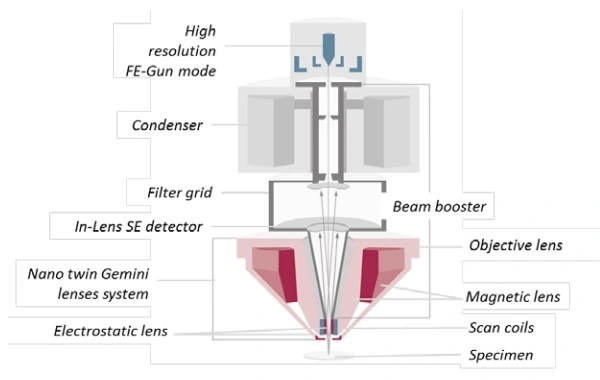
The method of operation of these microscopes is similar to that of conventional scanning electron microscopes (SEM). An electron beam focused by electromagnetic lenses scans the surface of specimen, where the reflected/interacted electrons create an image of the sample surface and topography (Figure 1).
FESEM Working Principles
The Difference between SEM and FE-SEM
In general, FESEM follows the same principles as the one in SEM, while the biggest difference between SEM and FE-SEM is the electron generation system. FE-SEMs use a Field Emission Gun (FEG) as electron source. In FEGs a potential gradient is applied to emit the electron beam, while in SEM thermionic emission is used.
How Does Field Emission Work in Field Emission Scanning Electron Microscopy (FE-SEM)?
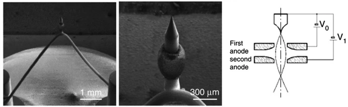
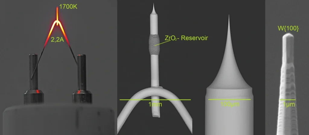
Field emission in FE-SEM is performed by FEGs through applying low voltages on an electron source, usually a single tungsten filament with a pointed sharp tip (Figure 2), which concentrates low-energy and high-energy electrons at a low electrical potential (about 0.02 to 5 kV) and increased spatial resolution. This method prevents contaminating the sample surface since does not require thermal energy to overcome the surface potential.
Field Emission Guns (FEG)
Field emission guns in FESEM imaging are divided into three types:
- Cold field Emission (CFE) Source
In CFEs the electron emission functions at room temperature and depends only on the electric field applied between the electrodes, using tungsten single crystal emitters. Although the current of the emitted electron beam is low, high brightness can be achieved due to the small diameter of the electron beam and emission area. This kind of FEG requires high vacuum condition to operate, otherwise, after a long operation period, adsorbed gas molecules on the FE-SEM tip will form a layer and can result in unstable current emission.
- Thermal Field Emission (TFE) Source
TFE guns operate at high temperature (1800K), which minimizes the adsorption of gas molecules on the gun tip and the stability of electron emission is improved even in lower vacuum conditions.
- Schottky Emission (SC) Source
SC has a larger electron sources compared to CFE at similar supplied energy, which enabled SC guns to prevent vibrations. This guns can utilize emitters of tungsten single crystals coated in zirconium oxide.
Sample Preparation
As sample preparation in SEM, surface of the FE-SEM samples should be conductive to reduce charging effects of the samples and improve image quality. In the case of insulating specimen, coating its surface with a thin film of a conductive material with a minimum thickness (0.5 to 3 nm), containing fine grain size smaller than the probe diameter, improves image contrast in low-density materials without affecting the sample appearance.

For effect of thin film grain size on the imaging quality please visit our blog article on the Effect of Base Pressure on Thin Film Grain Size in Sputtering.
FESEM vs SEM: Benefits and Limitations
- Thermionic emission of the electrons result in the substrate contamination, not occurring in the field emission electron sources
- In the SEM method, a resolution of 3-7 nm is achievable, while in the FE-SEM the resolution is 1.5 nm or better
- The conductive layer coated on a sample to be subsequently imaged by FE-SEM must be very thin and uniform and have finer grain size compared to what is required for SEM imaging
- Better contrast in low-density materials imaging through FE SEM technique is possible
- In FESEM, the electron source requires higher vacuum environment (higher than 10-9 Torr) during operation to ensure electron stability and prevent contamination of the cathode
- FE-SEM electron sources suffer low beam current stability
FESEM Applications
- Measurement of sample microscopic features
- Study of surface morphology
- Characterization of coatings
- Integrated circuit evaluation
- Fine structure analysis
- Study of microstructures
- Fracture and structural defects analysis
Our Coaters and FE SEM
Vac Coat SEM coaters are among the most favorable coating systems used for sample preparation for SEM and FESEM characterization. VacCoat offers semi/full automatic rotary pumped deposition systems (DSR1, DSCR, and DCR) for low vacuum deposition (You can read more about rotary pump and how to make the most efficient rotary pumps here) and turbo pumped coating systems (DST1, DSCT, and DCT) working at high vacuum with high precision thickness measurement and real-time monitoring of the process parameters, to improve deposition repeatability and accuracy (Read more about turbomolecular pump and turbomolecular pump protection here).
Vac Coat also provides coating devices with wider applications, such as DST3-T sputtering system plus thermal deposition with turbomolecular pump, to deposit composite layers of conducting and semi-conducting materials through DC/RF sputtering and thermal evaporation (Read more detail of RF and DC Sputtering here).
References
https://en.wikipedia.org/wiki/Field_emission_gun
Abd Mutalib, M., et al. “Scanning electron microscopy (SEM) and energy-dispersive X-ray (EDX) spectroscopy.” Membrane characterization. Elsevier, 2017. 161-179.
https://sites.google.com/site/quantummechanics16/home/electron-microscope
https://blog.phenom-world.com/sem-electrons
https://en.wikipedia.org/wiki/Scanning_electron_microscope
https://en.wikipedia.org/wiki/Field-emission_microscopy
Rohaida, C. H., et al. “Field Emission Scanning Electron Microscope (Fe-Sem) Facility in Bti.” Mater. Charact (2016).
Akhtar, K., Khan, S.A., Khan, S.B., Asiri, A.M. (2018). Scanning Electron Microscopy: Principle and Applications in Nanomaterials Characterization. In: Sharma, S. (eds) Handbook of Materials Characterization. Springer, Cham.https://doi.org/10.1007/978-3-319-92955-2_4
https://www.mee-inc.com/laboratory-expertise/field-emission-sem-fesem/