Reactive Sputter Deposition Conference 2025 (RSD 2025)
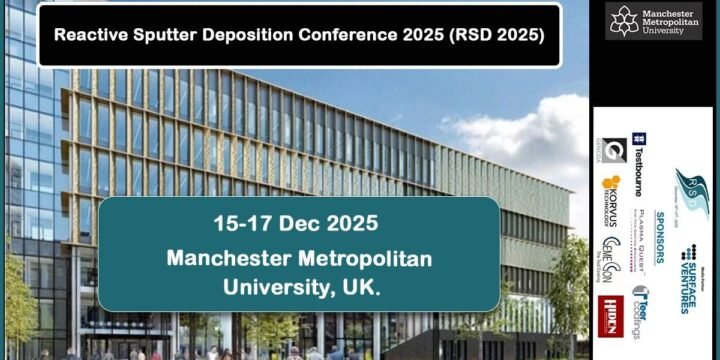
[vc_row][vc_column width="3/4"][vc_row_inner][vc_column_inner][vc_column_text css=""] Reactive Sputter Deposition Conference 2025 (RSD 2025) The International Symposium on Reactive Sputter Deposition (RSD 2025) is one of the most important professional events in the field of physical vapour deposition, thin film growth, and in particular reactive sputtering technology. The conference will be held on Tuesday 16 and Wednesday 17 December, 2025, at Manchester Metropolitan University, UK. [/vc_column_text][/vc_column_inner][/vc_row_inner][vc_row_inner css=".vc_custom_1765540499688{background-color: #D9D9D9 !important;}"][vc_column_inner width="1/2"][vc_cta h2="" txt_align="center" style="3d" color="mulled-wine" add_button="bottom" btn_title="Reactive Sputtering" btn_style="3d" btn_color="juicy-pink" btn_align="center" css="" btn_link="url:https%3A%2F%2Fvaccoat.com%2Fblog%2Freactive-sputtering%2F|title:Reactive%20Sputtering%3A%20A%20Brief%20Overview%20and%20Advantages"][/vc_cta][/vc_column_inner][vc_column_inner width="1/2"][vc_cta h2="" txt_align="center" style="3d" color="mulled-wine" add_button="bottom" btn_title="What is Thin Film?" btn_style="3d" btn_color="juicy-pink" btn_align="center" css="" btn_link="url:https%3A%2F%2Fvaccoat.com%2Fblog%2Fthin-film-and-thin-films-types%2F|title:Thin%20Films%20Coating%20and%20Applications"][/vc_cta][/vc_column_inner][/vc_row_inner][vc_row_inner][vc_column_inner][vc_column_text css=""] Also, a specialized training workshop has been designed for researchers, students and engineers, aiming to create a deeper understanding of the physical principles, laboratory methods and practical challenges of reactive sputtering deposition such as process control,…