HOW DOES QUARTZ CRYSTAL WORK?

HOW DOES QUARTZ CRYSTAL WORK?

Carbon Coater, Pulsed Laser deposition, Sputter Coater, Thermal evaporation
[vc_row][vc_column width="1/4"][vc_row_inner][vc_column_inner][vc_column_text] [lwptoc backgroundColor="#d6d6d6" borderColor="#5b5b5b" skipHeadingText="Recent Posts"] [/vc_column_text][/vc_column_inner][/vc_row_inner][vc_wp_posts number="5"][/vc_column][vc_column width="3/4"][vc_column_text] Solid materials whose atoms or molecules are regularly and repeatedly called crystals (the structure of these cells has a unit cell). Piezoelectric materials are electrically neutral and although the structures of the atoms of these materials are not symmetric, they neutralize each other in terms of electric charge. When a mechanical force is drawn into the piezoelectric material, the distance between the atoms is changed, and they move away from each other or together. As a result, the balance of electrical charges is mixed up and a net positive or negative charge is generated. On the other hand, when an electric current is given to the crystal it starts to oscillate. The frequency of the oscillation is depending on the…
Read More
Impact of Bias Voltage on Sputtering and SEM

Impact of Bias Voltage on Sputtering and SEM

Carbon Coater, Pulsed Laser deposition, Sputter Coater, Thermal evaporation
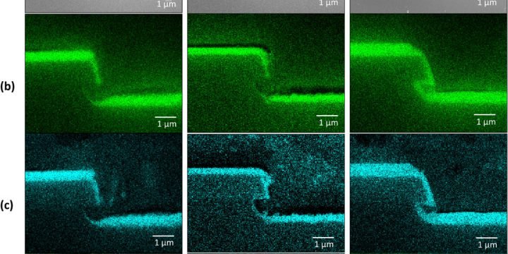
[vc_row][vc_column width="3/4"][vc_row_inner][vc_column_inner][vc_column_text] Impact of Bias Voltage on Sputtering and Scanning Electron Microscopy (SEM) The substrate bias voltage is applied to improvement of the directionality and energy of arriving particle to the substrate surface. It can modify the arrival characteristics of these particles such as direction and kinetic energy. As the direction and kinetic energy are controlled, greater penetration into high aspect ratio structures could be reached. [/vc_column_text][/vc_column_inner][/vc_row_inner][vc_row_inner][vc_column_inner width="1/2"][vc_cta h2="" txt_align="center" style="3d" color="mulled-wine" add_button="bottom" btn_title="What is SEM?" btn_style="3d" btn_color="juicy-pink" btn_align="center" btn_link="url:https%3A%2F%2Fvaccoat.com%2Fblog%2Fscanning-electron-microscope-sem%2F|title:Scanning%20Electron%20Microscope%20(SEM)|target:_blank"] [/vc_cta][/vc_column_inner][vc_column_inner width="1/2"][vc_cta h2="" txt_align="center" style="3d" color="mulled-wine" add_button="bottom" btn_title="Know more about Thin Films" btn_style="3d" btn_color="juicy-pink" btn_align="center" btn_link="url:https%3A%2F%2Fvaccoat.com%2Fblog%2Fthin-film-and-thin-films-types%2F|title:Thin%20Films%20Coating%20and%20Applications|target:_blank"] [/vc_cta][/vc_column_inner][/vc_row_inner][vc_separator][vc_row_inner][vc_column_inner][vc_column_text] On the other hand, collision of the particles which have sufficient energy with the deposited film could cause re-sputtering of the deposited layer. As a result, angular distribution of the deposited material could…
Read More