Sputtering Target Erosion- How to Enhance Sputter Target Utility?
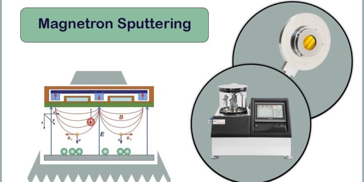
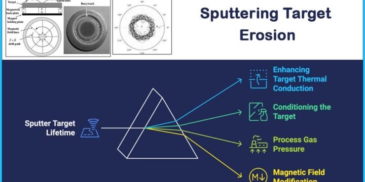
[vc_row][vc_column width="3/4"][vc_row_inner][vc_column_inner][vc_column_text css=""] Sputtering Target Erosion The sputter target surface undergoes erosion by successive collisions of the energetic charged particles through the magnetron sputtering process. The erosion pattern plays an important role in the sputter target lifetime or target utility; the more uniform the target erosion, the better the target utility. The target erosion patterns can be affected by several parameters, including the magnetic field over the target, geometrical properties of the target and the chamber, sputter process parameters, etc., which also influence the uniformity of the deposited layer by the coating process. [/vc_column_text][/vc_column_inner][/vc_row_inner][vc_row_inner css=".vc_custom_1770854183292{background-color: #D9D9D9 !important;}"][vc_column_inner width="1/2"][vc_cta h2="" txt_align="center" style="3d" color="mulled-wine" add_button="bottom" btn_title="More" btn_style="3d" btn_color="juicy-pink" btn_align="center" css="" btn_link="url:https%3A%2F%2Fvaccoat.com%2Fblog%2Fmagnetron-sputtering%2F|title:Magnetron%20Sputtering"][/vc_cta][/vc_column_inner][vc_column_inner width="1/2"][vc_cta h2="" txt_align="center" style="3d" color="mulled-wine" add_button="bottom" btn_title="Sputtering Targets" btn_style="3d" btn_color="juicy-pink" btn_align="center" css="" btn_link="url:https%3A%2F%2Fvaccoat.com%2Fsputtering-targets%2F|title:Sputtering%20Targets"][/vc_cta][/vc_column_inner][/vc_row_inner][vc_row_inner][vc_column_inner][vc_column_text css=""] What is Target Erosion? A sputtering target…


