Reactive Sputtering: Principles, Properties, Applications, and Challenges
Reactive sputtering is a versatile physical vapor deposition (PVD) technique employed in the sputter deposition of compound thin films by introducing reactive gases into the sputtering chamber. This article provides a detailed overview of the reactive sputtering process, including its underlying principles, operational modes, advantages, challenges, and diverse applications across various industries.
The article also delves into the critical parameters influencing the reactive sputtering process within a sputter coater, such as gas flow rates, pressure, and sputter power, along with strategies for optimizing film properties and addressing common issues like target poisoning and hysteresis effects.
1. What is Reactive Sputtering?
Thin films play a pivotal role in numerous technological applications, ranging from microelectronics and optics to energy storage and biomedical devices. The ability to precisely control the composition, microstructure, and properties of thin films is paramount to achieving desired functionalities and performance.
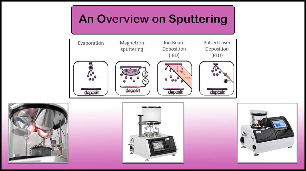
Among the various thin film deposition techniques, sputtering stands out as a versatile and widely used method due to its ability to deposit a broad range of materials with good adhesion and uniformity. The sputter coating process itself allows for robust and reliable film formation.


Reactive sputter deposition is a variant of conventional sputter coating that involves introducing reactive gases, such as oxygen, nitrogen, or methane, into the sputtering chamber of a sputter coater along with an inert gas, typically argon. The reactive gas reacts with the sputtered atoms from the target material, forming a compound that is then deposited as a thin film on the substrate.
This process enables the synthesis of a wide range of compound materials with tailored properties, including oxides, nitrides, carbides, and other complex compounds. This represents a core method of thin film deposition using physical vapor deposition.
Reactive sputtering process offers several advantages over other thin film deposition techniques, including precise control over film stoichiometry, high film density and uniformity, and the ability to deposit materials with complex compositions. However, the process also presents several challenges, such as target poisoning, hysteresis effects, and process instability, which require careful optimization and control within a sputter coater. RF sputtering is often used to mitigate some of these issues.


2. Principles of Reactive Sputtering
The reactive sputtering process, fundamental to thin film deposition, involves the following key steps within a sputter coating chamber:
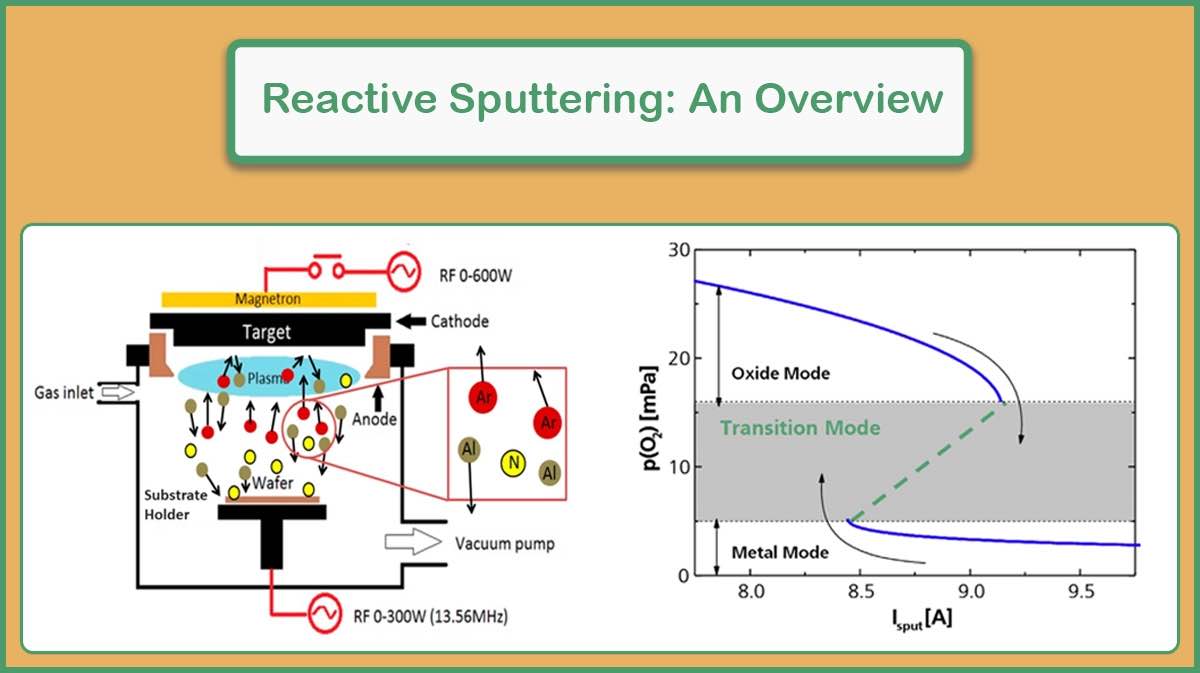
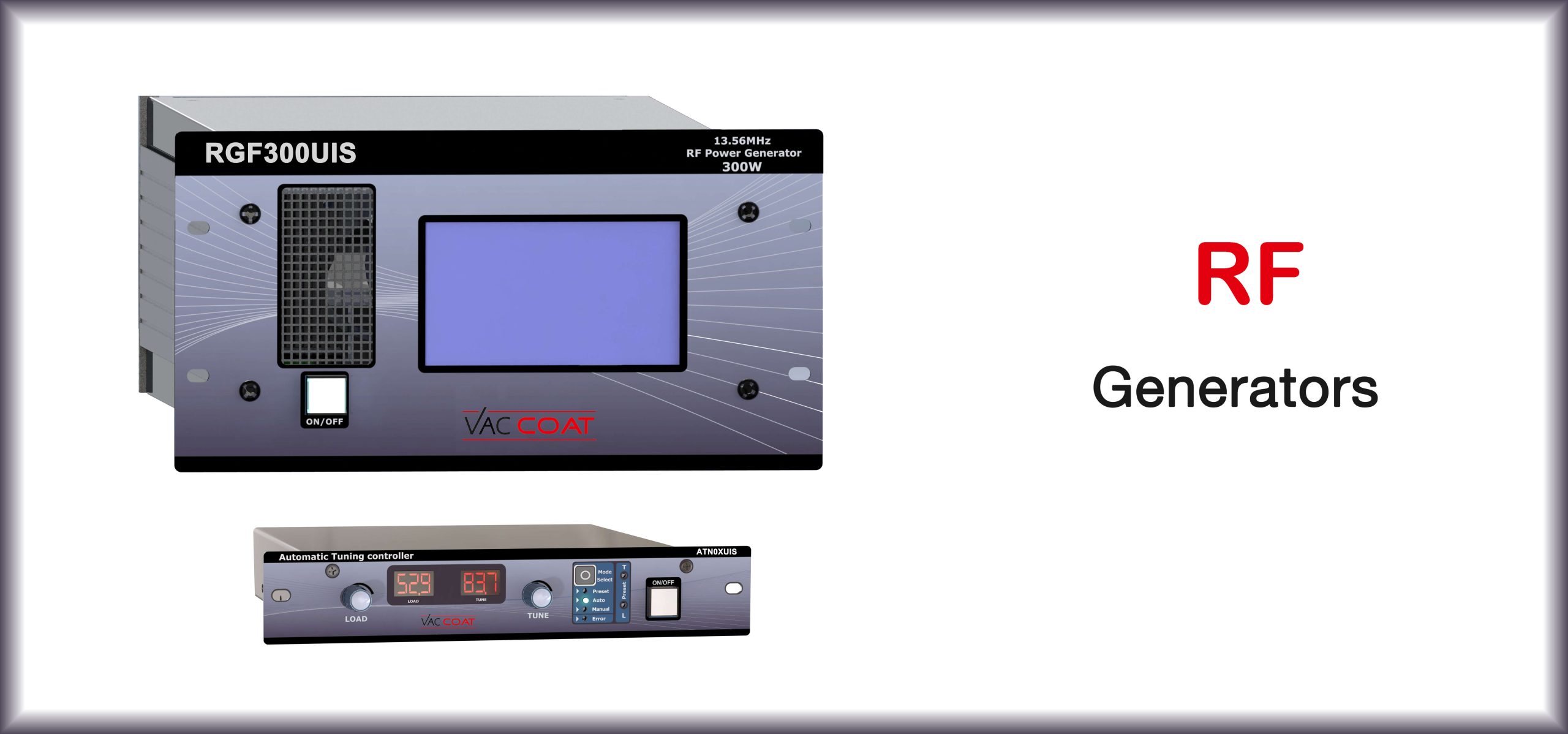
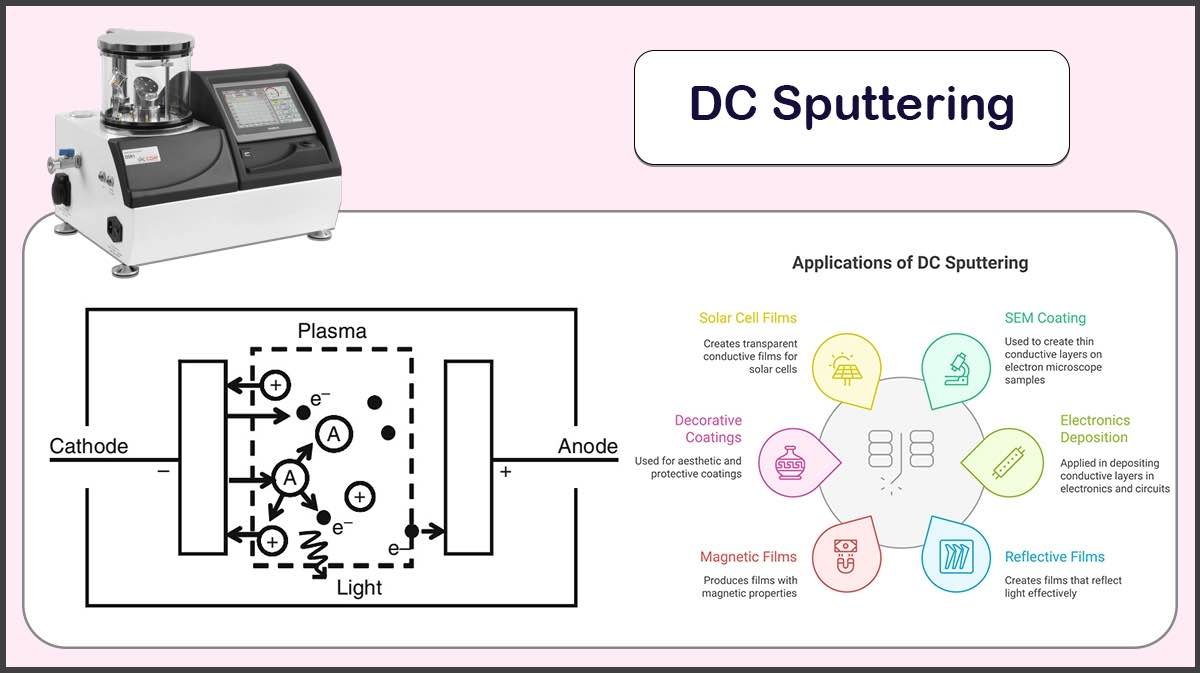
1. Plasma Generation: An inert gas, usually argon, is introduced into the vacuum chamber of the sputter coater and ionized by applying a radio frequency (RF sputtering) or direct current (DC) power source. This creates a plasma, which consists of positively charged ions, electrons, and neutral atoms.
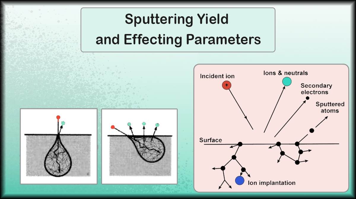
2. Target Sputtering: The positively charged argon ions are accelerated towards the target material, which is negatively biased. The energetic ions bombard the target surface, causing atoms to be ejected through momentum transfer. This process is known as sputtering, central to the sputter coating process.

3. Reactive Gas Introduction: A reactive gas, such as oxygen, nitrogen, or methane, is introduced into the vacuum chamber of the sputter coater at a controlled flow rate.
4. Compound Formation: The sputtered atoms from the target material react with the reactive gas either in the plasma or on the substrate surface, forming a compound. The stoichiometry of the compound can be controlled by adjusting the flow rates of the inert and reactive gases within the deposition chamber.
5. Film Deposition: The compound formed by the reaction between the sputtered atoms and the reactive gas is deposited onto the substrate, forming a thin film. This completes the sputter coating process.

3. Reactive Sputtering Modes
Reactive sputtering process in a sputter coater can operate in three distinct modes, each characterized by different process conditions and resulting film properties:

- Metallic Mode: In this mode, the reactive gas concentration is kept low, ensuring that the target surface remains predominantly in its metallic state. The deposition rate is relatively high, but the resulting film may not be fully stoichiometric, potentially leading to deviations from the desired compound composition.
- Transition Mode: This mode represents a balanced state where both the target and the substrate undergo partial reaction with the reactive gas. The transition mode is often preferred as it allows for achieving good film quality with acceptable deposition rates. Careful control of process parameters within the sputter coater is crucial in this mode to maintain stability and achieve the desired film properties.

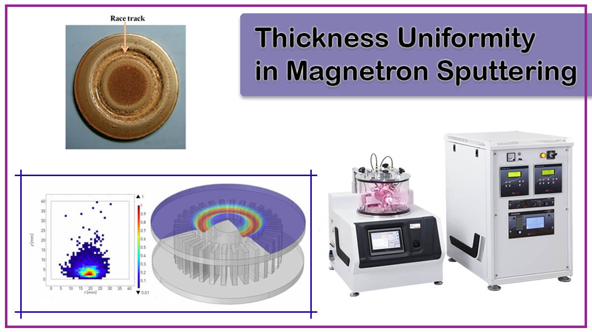
- Poisoned Mode: In this mode, a high reactive gas concentration leads to the formation of an insulating compound layer on the target surface, a phenomenon known as “target poisoning”.
This insulating layer reduces the sputtering yield and deposition rate, making the process less efficient. Furthermore, the poisoned mode is characterized by hysteresis effects, which can lead to process instability and make it challenging to control the film composition and properties, especially when compared to RF sputtering techniques.
The deposition rate of the film produced in the metallic mode (aD Me) is 3-4 times compared to the compound (aD,com) deposition rate in the reactive mode, as shown in Figure 3.

4. Advantages of Reactive Sputtering
Reactive sputtering as a physical vapor deposition technique, offers several advantages over other thin film deposition techniques:
- Stoichiometry Control: Precise control over the film’s stoichiometry is achievable by adjusting the reactive gas flow rate within the ion sputtering chamber. This allows for tailoring the film’s properties to meet specific application requirements.
- Versatility: Reactive sputtering can be used to deposit a wide range of compound thin films of materials, including oxides, nitrides, carbides, and other complex materials.


- High-Quality Films: The reactive sputtering process is capable of producing dense, adherent, and uniform thin films with controlled thickness and microstructure.
- Tailored Properties: By controlling the film’s composition and microstructure, its properties, such as hardness, optical properties, electrical conductivity, and chemical resistance, can be tailored for specific applications.
- Wide Range of Materials: Reactive sputter deposition applies to a broad spectrum of materials, including metals, semiconductors, and insulators. It can be used to deposit films on various substrates, including glass, ceramics, polymers, and semiconductors. The use of RF sputtering further expands the range of materials that can be deposited.
5. Challenges in Reactive Sputtering
Despite its advantages as a thin film deposition method, reactive sputtering presents several challenges that must be addressed to achieve optimal film properties and process stability:
- Process Complexity: Reactive sputtering is more complex than traditional sputtering due to the need to control the reactive gas flow and manage the chemical reactions occurring in the plasma and on the substrate surface within the coating chamber.
- Target Poisoning: The reactive gas can react with the target surface, forming a compound layer that reduces the sputtering rate and alters the film properties. This phenomenon, known as “target poisoning,” can lead to process instability and make it challenging to control the film composition.
- Hysteresis Effects: The relationship between the reactive gas flow and the film properties can be non-linear, leading to hysteresis effects that make process control challenging. Hysteresis occurs when the film properties depend not only on the current process parameters but also on the history of the process.
- Process Instability: Reactive sputtering processes can be prone to instability, with small variations in gas pressure, temperature, or power leading to abrupt changes in film composition and properties.
- Lower Deposition Rates: Reactive sputtering processes often exhibit lower deposition rates compared to non-reactive sputtering due to target poisoning and gas-phase reactions, especially if RF sputtering is not employed.
6. Strategies for Overcoming Challenges
Several strategies have been developed to address the challenges associated with reactive sputtering process and improve process control and thin film deposition quality:
- Process Control Techniques: Advanced process control techniques, such as voltage or optical monitoring, can be used to stabilize the process and mitigate hysteresis effects. These techniques involve monitoring key process parameters and adjusting the reactive gas flow rate or power to maintain the desired film properties.
- Pulsed-DC or RF Power Supplies: Pulsed-DC or RF sputtering power supplies can reduce target poisoning and improve the sputtering rate of insulating targets. Pulsed-DC power supplies involve applying a series of short pulses of DC power to the target, which can help to prevent the formation of an insulating layer on the target surface. RF sputtering power supplies, on the other hand, use radio frequency alternating current to generate the plasma, which can effectively sputter insulating materials.
- Substrate Heating: Heating the substrate during thin film deposition can promote the diffusion of adatoms and improve film density and adhesion. Substrate heating can also influence the film’s microstructure and phase composition, allowing for tailoring its properties.
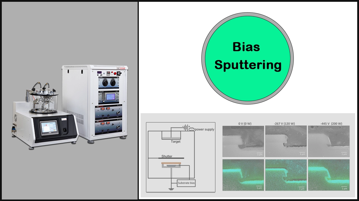
- Bias Voltage: Applying a bias voltage to the substrate can attract ions from the plasma and increase the kinetic energy of the depositing species, leading to denser and more adherent films during the sputter coating process. Substrate biasing can also influence the film’s stress state and preferred orientation.
- Pumping speed control: the hysteresis effect can be eliminated if SRG of the pumping system is greater than a critical value defined by some calculations. The turbo-pumped Vac Coat sputter coaters allow the user to control the turbo pumping speed for better optimization of deposition process.
- Target Design: Modified target designs, such as segmented targets or rotating targets, can help to reduce target poisoning and improve the sputtering rate. Segmented targets consist of multiple materials arranged in a specific pattern, while rotating targets continuously expose a fresh surface to the plasma, reducing the accumulation of insulating layers.

- Closed-Loop Control Systems: Implementing closed-loop control systems that automatically adjust process parameters based on real-time monitoring of film properties can improve process stability and film quality during thin film deposition. These systems typically involve sensors that measure film thickness -as in Vac Coat sputter coaters- composition, or other relevant properties, and a control algorithm that adjusts the reactive gas flow rate, power, or other process parameters to maintain the desired film properties.
- Dual-Cathode Designs: Dual-magnetron cathode sputtering systems can enhance plasma density and improve deposition rates, especially for reactive sputtering processes. Dual magnetron systems employ two magnetrons facing each other, creating a confined plasma region with high ionization efficiency.
- High-Power Impulse Magnetron Sputtering (HiPIMS): HiPIMS is a pulsed sputtering technique that uses high-power, short-duration pulses to generate a dense plasma with a high ionization fraction. HiPIMS can overcome the limitations of conventional DC and RF sputtering, such as low ionization efficiency and low deposition rates, making it suitable for depositing high-quality films with complex compositions.
7. Applications of Reactive Sputtering
Reactive sputtering has found widespread applications in various industries due to its versatility and ability to deposit a wide range of compound materials with tailored properties during thin film deposition. Some of the key applications include:
- Microelectronics: Reactive sputtering is used to deposit insulating layers (e.g., SiO2, Al2O3), transparent conductive oxides (TCOs) (e.g., ITO for displays), diffusion barriers, and other thin films essential for the fabrication of integrated circuits and microelectronic devices.
- Optics: Reactive sputtering is employed to produce anti-reflective coatings (e.g., MgF2), mirrors, optical filters, and other optical thin films with precise control over their refractive index and transmission properties.

- Hard Coatings: Reactive sputtering is used to deposit wear-resistant coatings for cutting tools (e.g., TiN, CrN), aerospace components, and other applications requiring high hardness and durability.
- Energy: Reactive sputtering plays a crucial role in the fabrication of thin-film solar cells (e.g., CIGS), fuel cell electrodes, battery coatings, and other energy-related devices.
- Decorative and Functional Coatings: Reactive sputtering is used to create gold-like TiN coatings for jewelry, scratch-resistant coatings for smartphones, and other decorative and functional coatings with enhanced aesthetic appeal and performance.

- Magnetic Storage: Reactive sputtering is employed to deposit ferromagnetic films (e.g., CoCrPt) for hard disk drives and other magnetic storage media.
- Packaging: Reactive sputtering is used to create gas/moisture barrier films for flexible electronics and food packaging, providing protection against environmental degradation and extending the shelf life of products.

All Vac Coat Sputter Coaters Flowchart.
8. Emerging Trends in Reactive Sputtering
Several emerging trends are shaping the future of reactive sputtering as a physical vapor deposition technique for thin film manufacturing:
- Advanced Plasma Diagnostics: The use of advanced plasma diagnostics, such as optical emission spectroscopy (OES), Langmuir probes, and mass spectrometry, is becoming increasingly common for real-time monitoring and control of reactive sputtering processes. These diagnostics provide valuable information about the plasma composition, density, and energy distribution, enabling better understanding and optimization of the sputter coating process.
- Hybrid Deposition Techniques: Combining reactive sputtering with other thin film deposition techniques, such as chemical vapor deposition (CVD) or atomic layer deposition (ALD), is gaining attention as a way to create novel thin-film materials with enhanced properties. These hybrid techniques allow for tailoring the film’s composition, microstructure, and interface properties with greater precision.
- Artificial Intelligence and Machine Learning: The application of artificial intelligence (AI) and machine learning (ML) algorithms to reactive sputtering is emerging as a promising approach for process optimization and control. AI/ML models can be trained on experimental data to predict film properties based on process parameters and optimize the sputter coating process in real-time.
- Reactive Sputtering for Nanomaterials Synthesis: Reactive sputtering is being explored as a versatile technique for the synthesis of nanomaterials, such as nanoparticles, nanowires, and nanotubes. By controlling the sputtering parameters and gas-phase reactions, it is possible to synthesize nanomaterials with tailored size, shape, and composition.
9. Conclusion
Reactive sputtering is a powerful and versatile technique for depositing compound thin films with controlled properties as a form of physical vapor deposition method. While the process can be more complex than standard sputtering due to issues like target poisoning and hysteresis, it remains a key technique in industries ranging from microelectronics to photovoltaics.
The ability to precisely control film stoichiometry, microstructure, and properties makes reactive sputtering an indispensable tool for creating high-performance thin films for a wide range of applications.
Advancements in process control techniques, power supplies, target designs, and plasma diagnostics continue to improve the reliability and efficiency of reactive sputtering, including RF sputtering, paving the way for new and exciting applications in the future of thin film deposition.
Some of Vac Coat Systems


References
- Musil, Jindrich, Jaroslav Vlcek, and Pavel Baroch. “Magnetron discharges for thin films plasma processing.” Materials Surface Processing by Directed Energy Techniques 1 (2006): 67-110.
- Bishop, Charles. Vacuum deposition onto webs, films and foils. William Andrew, 2011.
- https://en.wikipedia.org/wiki/Sputter_deposition
Licari, James J. Hybrid microcircuit technology handbook: materials, processes, design, testing and production. Chapter 3. Thin Film Processes, Elsevier, 1998.
Bräuer, G. “Magnetron sputtering.” (2014).
Sarkar, Jaydeep. “Sputtering and thin film deposition.” Sputtering Materials for VLSI and Thin Film Devices; Elsevier: Amsterdam, The Netherlands 2 (2014): 93-170.
- Iqbal, Abid, and Faisal Mohd-Yasin. “Reactive sputtering of aluminum nitride (002) thin films for piezoelectric applications: A review.” Sensors 18.6 (2018): 1797.