
What is DC Self-Bias Voltage?
DC self-bias voltage stems from greater electron mobility compared to the ion’s. A higher DC self-bias leads to an elevated rate of ion collision to the electrode, resulting in higher etching or sputtering performance. The sputtering rate from the target in RF sputtering is highly correlated to the DC self-bias voltage created on the target. The DC self-bias is developed by itself and it can be manipulated by effective parameters to form a stable plasma and create better coatings.

What Is the DC Self-Bias Voltage in RF Sputtering?
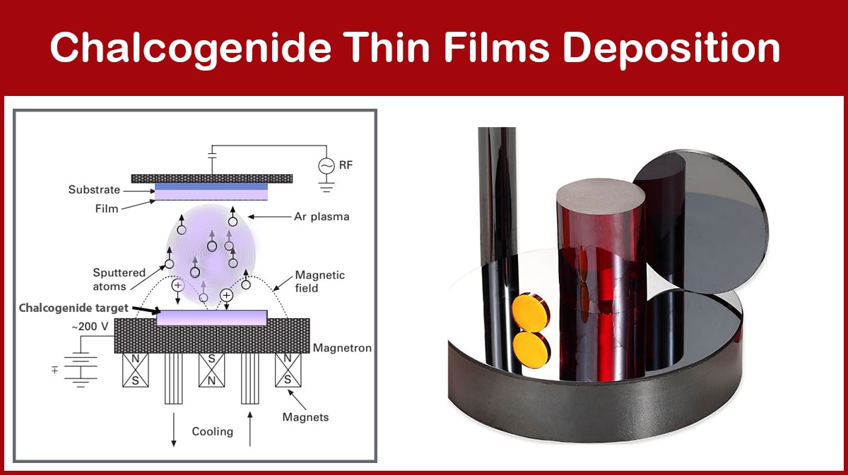
The sputtering process is preserved through the formation of plasma, the ionized gas between the two electrodes due to the high electric voltage difference, in which electrons and ions move freely without subatomic interactions.
During the sputtering process the plasma ions and electrons bombard the target surface, contributing to the ablation of target atoms. During RF sputtering, the electric pole of the target is regularly changed by an RF power generator, attracting the electrons and ions alternatively. The electrons are extremely lighter elements than ions and show higher mobilities (i.e., move much faster), hence collide the target more frequently during periodic change in the electric field, resulting in an excess negative charge on the target and DC field formation. The blocking capacitor in the RF matching network act as an isolator for this self-biased DC field, and the target acquires a negative DC bias.

DC Self-Bias Role in the Sputtering Rate
This DC self-bias is limited by the negative charge buildup, which leads to improved ion attraction onto the target. The enhanced ion-bombardment sputters the target atoms away for subsequent deposition on the substrate. The average energy of the ions corresponds to the overall DC self-bias (Vdc) and the plasma potential (Vpp).
Ion energy (eV) = -Vdc + Vpp
In a sputtering process, the consistent and uniform etching of the target strongly depends on the careful control over the level of RF power and the resulting DC bias. The chemical reactions of the process gas and the resulting compounds inside the vacuum coating chamber also affect the DC self-bias voltage.

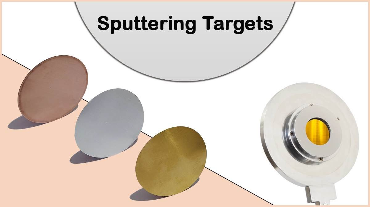
Sputter Deposition Target
The sputtering target is typically placed on the vacuum chamber’s lead (facing downward) and the substrate to be coated with a thin film is placed on a substrate holder beneath it, as in Vac Coat single cathode sputter coaters like DSR1 and DST1, or triple target sputter coater DST3. However, the target can be placed on the chamber baseplate (Facing upward), with the substrate holder above it, facing down, as in DST2–TG model.
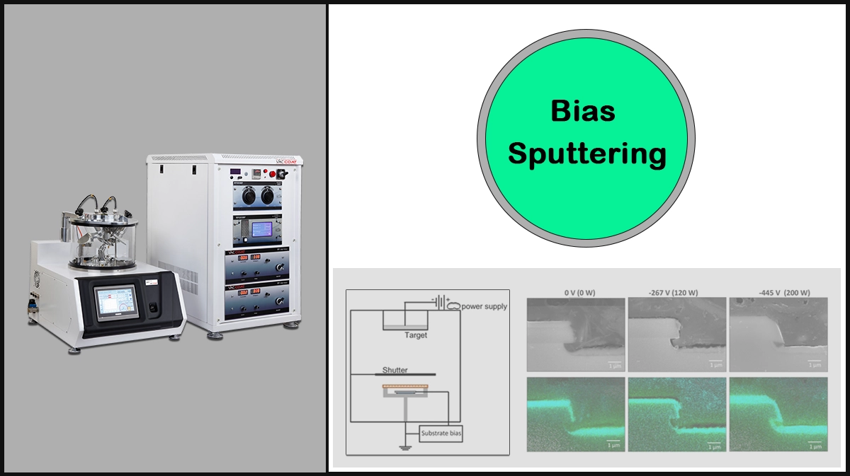
The target atoms may also be ionized, therefore will show better attraction to a negatively-biased substrate to form a thin film with desired structure and properties on it (For more information please visit Impact of Bias Voltage on Sputtering and SEM).


Influencing Parameters on the DC Self-Bias
Enhancing the self-bias voltage without changing the geometric factors of the deposition chamber, like target-to-substrate distance, results in an improved deposition rate. There are several factors that can highly influence the DC self-bias voltage during RF sputtering.
The factors that influence DC self-bias are:
- Ratio between the surface areas of the ground and powered electrodes, which is a fixed parameter for a previously designed chamber
- Chamber pressure
- RF deposition power
- Process gas composition
Chamber Pressure
The DC self-bias is inversely proportional to the chamber pressure. The vacuum level affects the deposition rate from different point of views. The more gas species inside the sputtering chamber, the smaller is the target material mean free path, so it reaches the substrate harder, according to the kinetic theory of gases. Therefore, the deposition chamber should be kept at higher vacuum levels to reach higher deposition rate. On the other hand, the electron’s mean free path also increases at lower pressures, which results in higher DC self-bias voltage. So DC self-bias voltage can be increased by reducing the chamber pressure. The increased self-bias leads to a higher sputtering rate.

RF Power
The DC self-bias is directly proportional to the RF forward power supplied by the RF plasma source. An increase in the RF power results in increasing the self-bias, as shown in Figure 3. The increase in the self-bias with the absorbed RF power can be contributed to the expansion of the plasma along with the RF voltage increase.


Process Gas Composition
The type of the process gas that is used in the plasma formation also affects the resulting DC self-bias. Figure 4 displays the self-bias voltages in different process gas compounds. Adding electronegative gases such as Cl2 increases the asymmetry in the RF plasma chamber. The Ar/Cl2 plasma contains electrons at higher temperature and lower electron density compared to the Ar plasma, consequently the self-bias voltage is higher in the Ar/Cl2 plasma.

Vac Coat RF Sputtering Systems
Vac Coat sputtering systems with large chamber can be equipped with RF signal generators to enable sputtering of the insulating or semiconducting targets. Vac Coat RF sputtering systems are provided with a matching network that shows the amount of the DC self-bias and can effectively tune the forward power of the RF power source to perform a reliable, repeatable deposition process.

Vac Coat offers high-vacuum DTE and DTT desk thermal evaporators optimized for the deposition of different materials’ thin films by thermal evaporation methods.
Vac Coat Ltd. offers different SEM coaters based on PVD techniques like sputtering, thermal evaporation, & carbon coating working at low/high vacuum conditions.
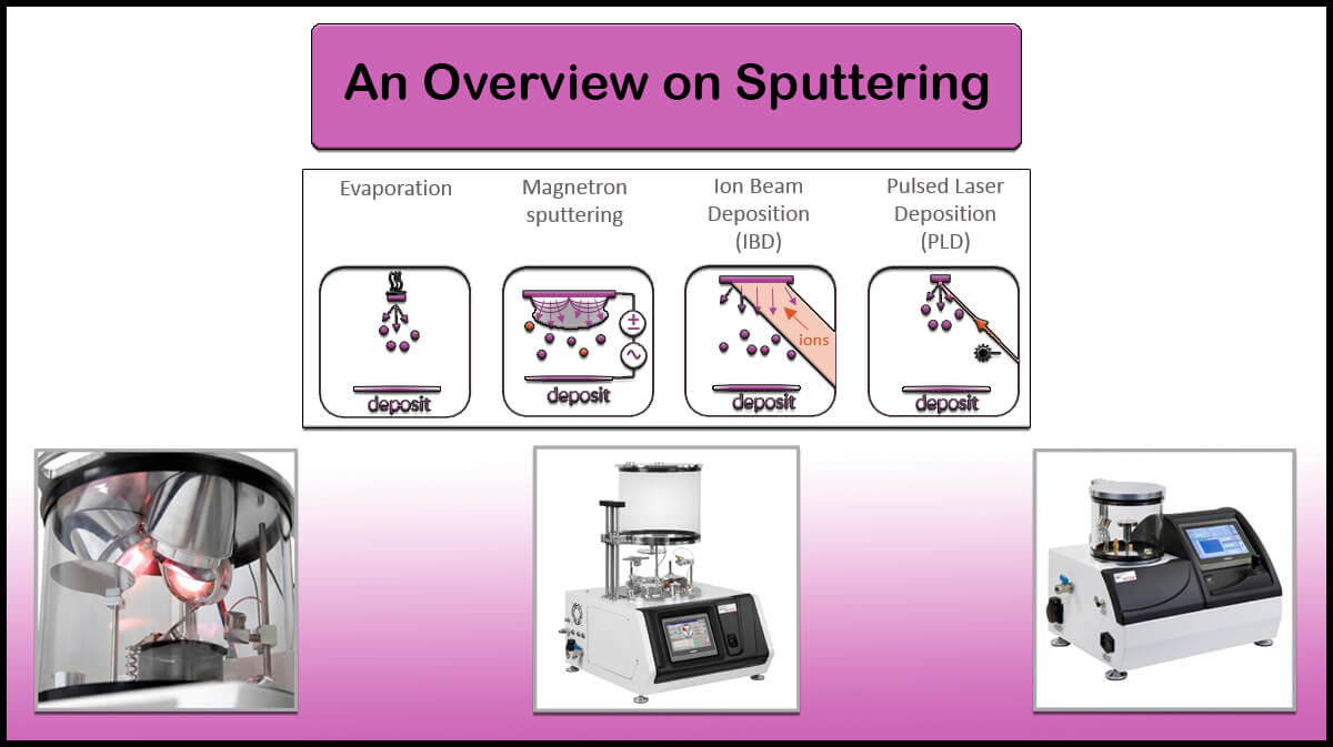
Vac Coat Ltd. produces and designs different types of sputter coaters systems. Sputtering is a method to deposit thin films of various materials on a substrate.


References
- Ohring, Milton, Sohrab Zarrabian, and Austin Grogan. “The materials science of thin films.” Appl. Opt 31.34 (1992): 7162.
- https://physics.stackexchange.com/questions/430948/rf-sputtering-where-comes-the-target-self-bias-voltage-from
- https://www.palomartechnologies.com/blog/the-importance-of-dc-self-bias-voltage-in-plasma-applications
- Nojiri, Dry Etching Technology for Semiconductors.
- M. J. Kushner, Monte-Carlo simulation of electron properties in RF parallel plate capacitively coupled discharges.
- J. Upadhyay, S. Popović, A.-M. Valente-Feliciano, L. Phillips and L. Vušković , Self-bias Dependence on Process Parameters in Asymmetric Cylindrical Coaxial Capacitively Coupled Plasma.