
Perovskite Solar Cells
Perovskite solar cells are a kind of solar cell that combines the structure of perovskite. This substance is often an organic-mineral hybrid of lead or tin halides. Perovskite materials such as methyl ammonium lead iodide are cheap and easy to make. The structure of perovskite is a triple structure of materials, and its general formula is ABO3. This structure consists of octahedrons, in which the cations A are located in octahedral cavities. The thin-film perovskite solar cells have high conversion efficiency and can be manufactured in cheap and cost-effective ways. Compared to silicon solar cells, which are usually made in multi-stage and expensive processes, perovskite solar cells can be constructed easily in laboratory conditions. These cells have been the fastest solar technology ever since.
The advantage of perovskite solar cells is the cost-effectiveness of raw materials and their adjustable band gap by changing the amount and proportion of the halide. The unique features of the perovskite, including the high absorption coefficient, make it possible to create a solar cell with thin films with a very low thickness (up to 500 nm). In other words, visible light can be completely absorbed by a thin layer of several hundred nanometers from the perovskite. The remarkable photovoltaic performance of hybrid perovskite has been attributed to their long carrier lifetime and the high impact of photoluminescence.
Perovskite’s growth conditions and deposition operation largely alter the layer morphology, carrier lifetime, and device performance. The best method for deposition of the optoelectronic instrumentation is vacuum evaporation-based method, which produces high-quality thin film while having environmental hazards and low costs. High mobility of the charge carriers and low recombination rate of carriers are the positive aspects of deposited layer using vacuum evaporation based deposition methods.

For the first time in 2009, perovskite was reported by Miasaka et al. The reported cell had a structure similar to pigment solar cell, with only 3.8% efficiency. In addition, the cell was stable for only a few minutes because of the use of corrosive electrolytes. A great success in this field came when Henry Snaith and Mike Lee from Oxford University found that perovskite was stable contacted with a solid-state hole transporter such as spiro-OMeTAD and did not require the mesoporous TiO2 layer in order to transport electrons.
They showed that efficiencies of almost 10% were achievable using the “sensitized” TiO2 architecture with the solid-state hole transporter, but higher efficiencies, above 10%, were attained by replacing it with an inert scaffold. At present, the highest efficiency of these cells is 22.7% .
Although primary solar cells with the n-i-p structure are still widely used, the inverse p-i-n structure has attracted increasing attention. Depending on the role of the perovskite layer in the cell or the nature of the upper and lower electrodes, perovskite solar cells are constructed in different structures. The two groups of these cells are “sensitized” solar cells and “thin film” solar cells. In the first category, perovskite has the role of absorbing light and the charges collected by another material. In the “thin film” perovskite solar cells, the electron and hole transport is done in the bulk perovskite.
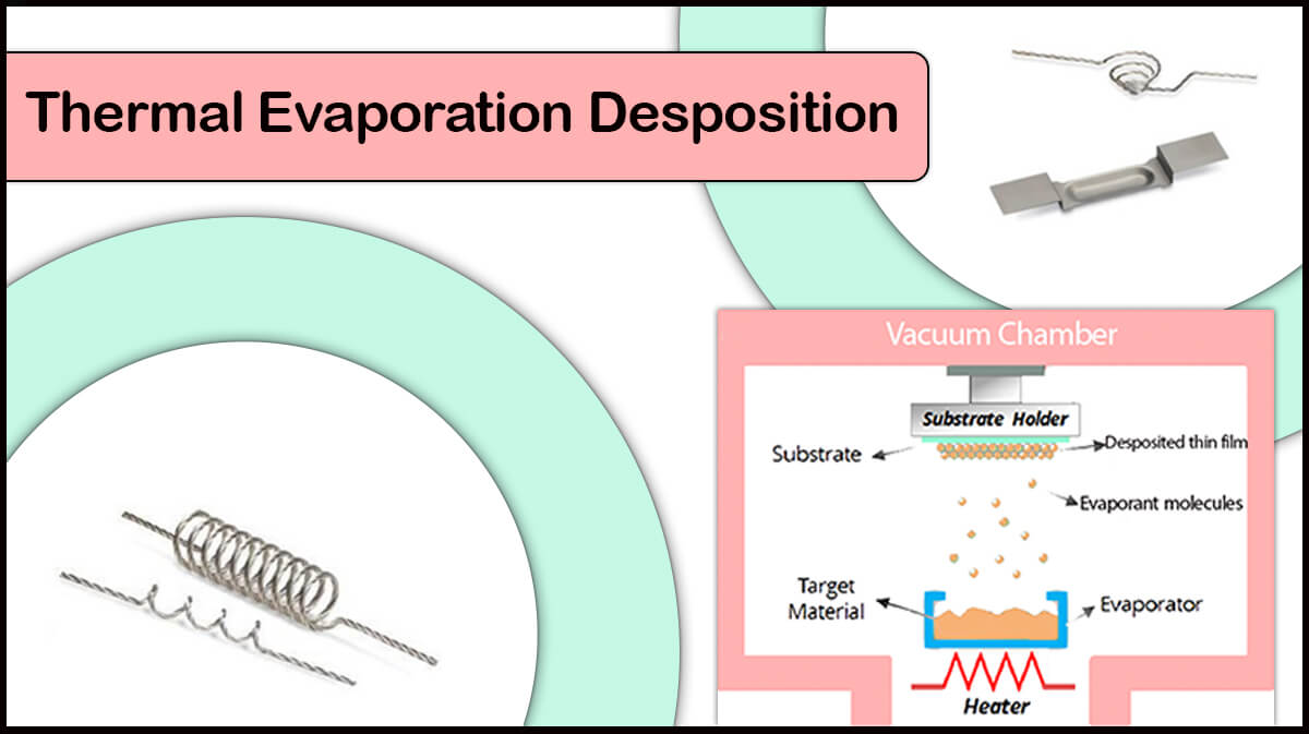
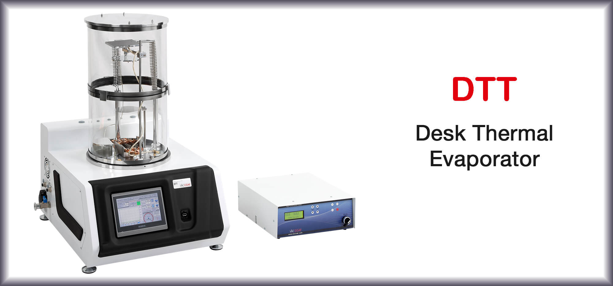
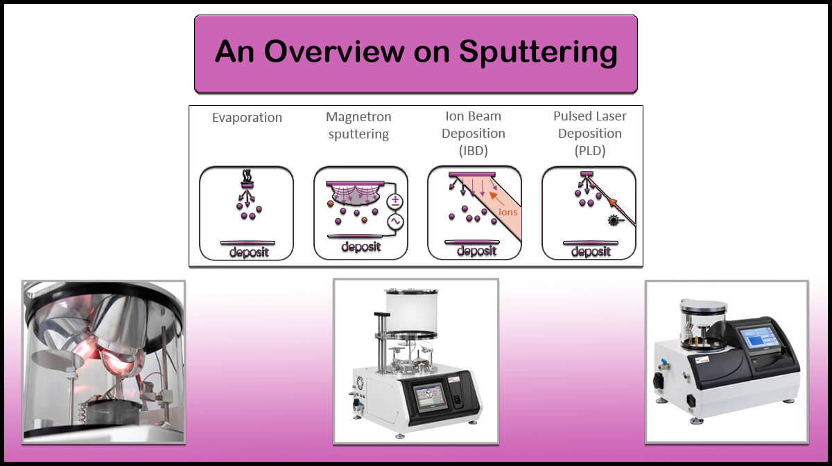
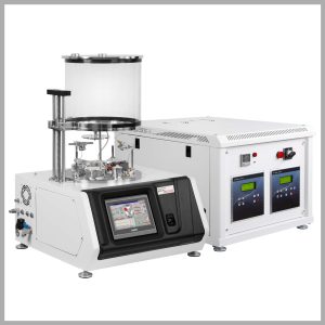
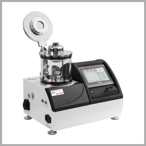
Different metals such as aluminum, silver or copper have already been used as electrodes in the perovskite solar cells, all of which are deposited by the thermal evaporation method. Among Vac Coat’s products, the DTT Vacuum Coater and Desk Sputter Coater – DST3-T are suitable to create these electrodes. The use of thermal evaporation method compared with other deposition methods such as sputtering deposition has led to deposition of the electrodes which improve the conversion efficiency of the perovskite solar cells, thereby improving the performance of the thin film perovskite solar cell.
According to the research conducted by German researchers in 2018, the aluminum electrode deposited by the thermal evaporation method is better than the aluminum electrodes deposited by the sputtering and electron beam (e-beam) methods.
Due to the inevitable damage to the interface of the electrodes with organic electronic transfer layer (ETL), resulting from the direct deposition of the electrode layer onto the organic layers (BCP/PCBM) with electron beam (e-beam) or sputtering deposition methods, the current-voltage curve of the perovskite solar cell change to S-shaped.
Although, a short heating stage in the temperature range of 30 to 100°C can remove the damage which lead to the S-shaped current-voltage curve caused by the electrode deposition by the e-beam or sputtering method. The damage results in the disorder of surface molecules that prevent electrons from exiting and causing charge accumulation on the surface. The imbalance of the carriers on both sides of the interface creates a shape S in the voltage-current curve.
In the case of e-beam, an electron beam is concentrated by the magnetic field on the material (Al) and converts it from solid state to gas by electron energy transfer. The damage caused at the interface between the electrode and the organic electronic transfer layer (ETL) is due to the deviation or reflection of high-energy electrons from the electron beam (e-beam).
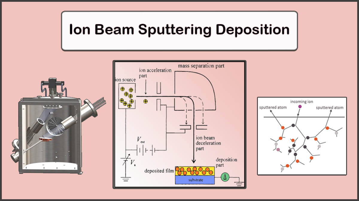
In the case of the sputtering deposition, Aluminum atoms come out of the target. The sputtering process is that when argon plasma is formed between the target and the substrate, the positive ions of the argon are accelerated to the target with enough energy to separate the aluminum atoms, and collide with the aluminum target. The energy transmitted to the metal particles in the sputtering process is much greater than the energy transferred to it in the process of thermal evaporation or the electron beam (e-beam) deposition which leads to a denser electrodes deposition than the other two methods.
The damaging effect of this method is due to the interaction of plasma particles (including neutral argon particles, high energy electrons and charged ions) into the organic electronic transport layer (ETL). This damage is worse than can be solved by the annealing process.
If a high-energy sputtering process is used to form a denser electrodes layer, the shape S will be observed in the current-voltage curve even, after several annealing stages. According to researchers, perovskite solar cells with aluminum electrodes deposited with all three methods of sputtering, electron beam (e-beam) and thermal evaporation have a yield of more than 11 percent, but the parameters of these solar cells are different. In overall, the best results are related to the perovskite solar cell whose electrode is deposited using the thermal evaporation method.

Some of Vac Coat Products
To find out more and to get the exact results of this research, see the bellow links:
References
- Manser, Joseph S. and Christians, Jeffrey A. and Kamat, Prashant V. (2016). “Intriguing Optoelectronic Properties of Metal Halide Perovskites”. Chemical Reviews. 116 (21): 12956–13008. doi:10.1021/acs.chemrev.6b00136
- Charge-carrier dynamics in vapour-deposited films of the organolead halide perovskite CH3NH3PbI3xClx, Christian Wehrenfennig, Mingzhen Liu, Henry J. Snaith, Michael B. Johnston and Laura M. Herz, Energy Environ. Sci., 2014, 7, 2269–2275.
- Kojima, Akihiro; Teshima, Kenjiro; Shirai, Yasuo; Miyasaka, Tsutomu (May 6, 2009). “Organometal Halide Perovskites as Visible-Light Sensitizers for Photovoltaic Cells”. Journal of the American Chemical Society. 131 (17): 6050–6051. doi:10.1021/ja809598r.
- Comparison of the Al back contact deposited by sputtering, e-beam, or thermal evaporation for inverted perovskite solar cells, Tina Wahl, Jonas Hanisch, and Erik Ahlswede, Journal of Physics D: Applied Physics, 2018.
- https://doi.org/10.1088/1361-6463/aab0d8








Interesting overview! It would be great to see more detail about how perovskite cells can be integrated into flexible or lightweight solar panels.