Transmission Electron Microscopy (TEM)
Conventional transmission electron microscopy (TEM) utilises a beam of electrons interacting with a thin specimen. The scattered electrons transmitted through the sample are subsequently collected to form an image revealing its structure. Transmission electron microscopes are consistently developed to overcome challenges and enhance the image resolution below 1 nm and magnification of up to 1,000,000x, creating various modes for extensive applications, such as high-resolution imaging of micro-nano structures, crystalline phase orientations, and elemental analysis.
Moreover, achieving high-quality, accurate results for electron microscopy, specifically TEM, requires considerations in sample preparation steps prior to the analysis. This article is intended to shed light on the transmission electron microscopy basics, components, modes, as well as its applications, advantages, and challenges.
Transmission Electron Microscope’s Components
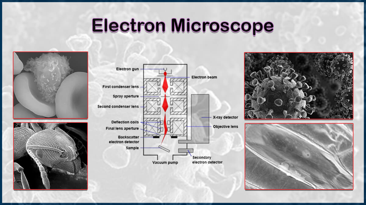
A typical transmission electron microscope should contain several parts. Briefly, a steady beam of electrons is generated in a vacuum environment, going through a microscope column containing electromagnetic lenses and apertures inside a TEM. The transmitted beam from the specimen is then collected by various detectors, including imaging cameras and spectrometers, and the resulting data is further analysed through the proper software. Some parts of a TEM are introduced below:
- Electron source: Cold field-emission guns (FEGs) and Schottky FEGs can be used to emit a stable beam of electrons with a uniform energy distribution.
- Vacuum system: A high vacuum system is required to increase the mean free path of the electron beam and lower the chance of unwanted electron collisions and data loss.
- Microscope Column: Includes electromagnetic lenses and apertures to control the beam diameter and focus, leading to controlled magnification and inspection of different parts of the sample.
- Detectors: Imaging cameras and different spectrometers can be utilised to reveal the structure and elemental composition of the sample.
What Happens in Electron-Sample Interactions?
The conventional TEM imaging results from the transmitted electrons through the sample are collected using the TEM aperture. When the electrons encounter the sample, part of the beam passes through the sample, resulting in the brighter regions of the image, which is called Bright-field (BF) imaging.
In transmission electron microscopy, the electrons passing through the specimen undergo electron-matter interactions and scattering. These interactions may lead to changes in different features of the electron beams, including amplitude (through Rutherford back scattering through collision with heavy atoms or Bragg diffraction), phase (resulting from destructive and constructive interference of multiple beams with relative phase shifts), etc.
Further structure and elemental analysis of the specimen can be deduced from the collected scattered electrons. Correspondingly, elastic and inelastic collisions happen according to the energy transfer between the electron and the matter.
Elastic and Inelastic Scatterings
In elastic collisions, there is no energy transfer between the electron and the matter, and the main interaction is through the change of path or phase of the electron beam.
When the electron beam energy is changed while passing through the specimen, an inelastic interaction occurs. These interactions give rise to atomic excitations of the sample and cause a measurable energy loss, as a result of emission of secondary electrons with characteristic energies corresponding to the atomic structure of the sample elements. This method is typically used to determine the sample elemental composition.
Transmission Electron Microscopy Techniques
Other than capturing transmitted electrons from the sample, as in conventional transmission electron microscopy, TEM imaging can be performed in different operating modes and employing various techniques to achieve the best result according to the sample under study and the required information. These modes are attainable through adjusting the parameters of different components of the microscope, including lenses or apertures.
In the following, some of the most practical TEM techniques are described.
A. TEM Dark-field Imaging:
In TEM dark-field imaging, an objective aperture is used to collect scattered electrons that pass through the specimen and blocks the transmitted ones. Hence, the crystal lattice structure details can be studied within this TEM technique.
Diffraction imaging
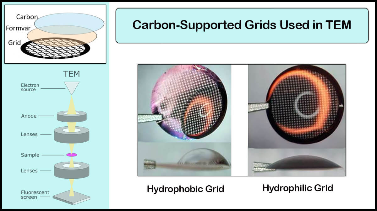
A diffraction pattern, such as Bragg diffraction, happens when the electron wavelength is comparable to the lattice crystalline spacing of the matter. Subsequently, parts of the electrons will scatter to specified (Bragg) angles. Collecting these electrons and blocking the transmitted ones provides an image where a dark sample in the foreground appears within a light background, Dark-field (DF) imaging, useful in studying biological structures, like viruses, bacteria, and cellular organelles sections which are supported over TEM grid holes coated with a thin plastic (like Formvar) that can be strengthened with carbon coating.
Selected Area Diffraction (SAD)
Using a SAD aperture and restricting the observing region, an image containing an array of dots or diffuse rings, depending on the sample crystalline structure, appears below the sample on the back focal plane, from which the crystal structure can be deduced.
Convergent Beam Electron Diffraction (CBED)
In CBED, the beam of electrons is converged onto a single point on the sample by adjusting the focus (Objective lens) rather than using the objective aperture, and the disc-like diffraction patterns containing the information on the sample’s crystal symmetry are recorded to determine the crystal point and space group.
B. High-Resolution TEM (HR-TEM)
The phase change between multiple transmitted and diffracted beams is used to generate contrast in high-resolution TEM imaging, which can be affected by microscope lens aberrations, including defocus, spherical aberration, and astigmatism. HR-TEM empowers direct visualisation of atomic structures in materials like semiconductors, metals, nanoparticles, and sp²-bonded carbon (e.g., graphene, carbon nanotubes). Capturing the two-dimensional spatial wave amplitude distribution, it is similar to a classic light microscope, with the highest resolution of about 0.5 Å (0.050 nm), which allows for the observation of individual atoms and defects in crystals.
For three-dimensional crystal imaging, multiple views from different angles are combined through a technique called electron tomography.

C. Scanning Transmission Electron Microscopy (STEM)
The STEM imaging technique allows using multiple correlated signals, involving scattered electrons, secondary electrons, and enables the use of other signals that cannot be spatially correlated in TEM, including secondary electrons, scattered beam electrons, characteristic X-rays, and electron energy loss, allowing very accurate elemental mapping and chemical analysis of samples.
Annular Dark-Field Imaging
This is a method for mapping samples’ structure in a scanning transmission electron microscope (STEM). STEM-Annular dark-field images are formed by collecting scattered electrons with an annular dark-field detector, unlike conventional TEM dark-field imaging that uses an objective aperture to differentiate the scattered electrons that pass through from the main beam. Consequently, more electrons are collected in this method, which results in enhanced contrast and signal collection efficiency, as well as allowing the main beam to be directed to an electron energy loss spectroscopy (EELS) detector. Annular dark-field imaging can also be performed in parallel with bright-field STEM imaging and dispersive X-ray spectroscopy (EDX) analysis.
High-Angle Annular Dark Field (HAADF) Images
HAADF is a STEM technique with a resolution better than 0.05 nm that captures quasielastically Rutherford scattered electrons at high scattering angles (Convergence semi-angle ~50-200 mrad) using an annular dark-field detector, compared to the semi-angle of about 25 mrad for a 200 kV typical TEM. The intensity of HAADF images correlates with the square of the atomic number, making heavy atoms appear brighter while light atoms are less visible, owing to larger electrostatic interactions between the atomic nucleus and the incident electron beam. Minimising multiple scattering with no interference effect provides an easier interpretation of the resulting images.
HAADF is sensitive to atomic number variations, producing Z-contrast images. This sensitivity makes it valuable for identifying high-Z elements in matrices of lighter elements (lower Z number), particularly in heterogeneous catalysis, to determine the metal particle sizes and distributions.
Unlike conventional dark-field imaging, HAADF does not use an aperture but collects scattered electrons through an annular detector, enhancing signal efficiency.
LAADF (Low-Angle Annular Dark-Field) and ABF (Annular Bright-Field)
LAADF and ABF are complementary techniques to HAADF, which help to make light elements of the sample visible by placing the corresponding detectors below the HAADF detector.


D. EELS and EDX
The electron energy-loss spectroscopy (EELS) and energy-dispersive X-ray spectroscopy (EDS or EDX) are among the various inelastic scattering examinations that can be executed during TEM imaging. In EELS, the energy loss of the incident electron beam is measured, while the characteristic X-rays of the sample materials are detected through energy-dispersive X-ray spectroscopy (EDS or EDX). In case of emission of lower energy photons, compared to X-rays, visible light can be observed, called the cathodoluminescence (CL) phenomenon.
The HAADF technique, in combination with the electron energy loss spectroscopy (EELS), can map the atomic column position of elements.
E. Correlative TEM
Correlative microscopy involves using multiple microscope systems to observe the same specimen, such as light microscopy or scanning electron microscopy, along with transmission electron microscopy.
F. Cryo-TEM
In the cryo-TEM technique, the biological specimens are studied while frozen, helping to visualise their macromolecular structure, like proteins, at sub-nanometer resolution, without the need for chemical fixation and damage to the sample.
Sample Preparation For TEM Imaging
The TEM sample preparation method strongly depends on the specimen’s properties. The sample under study can be in various shapes, such as powders, biological samples, hard or soft masses, and contain materials showing different interactions with the incident electron beam. Accordingly, several preparation steps are designed to meet the requirements to achieve high-resolution TEM imaging.
The TEM sample preparation techniques may include cutting, ion beam thinning (milling), dehydration, (Cryo-)ultramicrotomy, etching, polymerisation, creating a sample replica, and mounting on the grid, due to the sample features.

Sample Replica
In case of TEM imaging of beam-sensitive specimens, typically biological samples like viruses, fibres or enzymes, a thin layer of evaporated metal, such as platinum or gold, is applied on their surface. This process can be followed by coating a carbon layer to enhance the metal replica’s stability. Then, the fragile biological mass is dissolved in an acid bath, and the remaining replica is mounted onto the TEM grid.
TEM Grids Preparation
TEM grids with open slots or patterned meshes hold the TEM sample to effectively interact with the electron beam without interfering with the resulting signals. These grids are commonly coated with a thin plastic layer (Like Formvar) backed by a carbon coating to support the specimen on the grid.
TEM Applications
Transmission electron microscopy empowers imaging of micro and nano-structures, like thin films and epitaxial layers, superlattice wavelength, composition and thickness of deposited coatings, interface orientation, nanoparticles size measurement and distribution with atomic resolution, useful in various fields, like biological, medical, and materials science, studies of nanostructures and proteins, as well as geology and environmental science.
Moreover, TEM imaging enables phase identification of materials through selected area electron diffraction on secondary phases and crystal orientation relationship by diffraction patterns.
Furthermore, TEM is one of the main tools in nanoscale imaging and analysis of quantum materials in real and reciprocal space, to unleash their structure within sub-angstrom spatial resolution.
Chemical mapping of degraded grain boundaries to observe elemental diffusion at the interfaces as a result of corrosion and heating is another application of TEM analysis.
TEM: Advantages and Challenges
TEM Advantages
TEM imaging has various advantages over other microscopy techniques, including:
- The highest magnification and resolution
- Adaptable imaging modes: dark and bright field, as well as phase contrast and high-angle annular dark field (HAADF).
- Achieving structural and crystallographic information by producing electron diffraction patterns (Such as the SAD technique).
- Enabling chemical analysis of samples at the nano-scale for elemental composition and bonding structure.


Challenges of TEM Imaging
Besides the numerous strengths of the transmission electron microscopy, this technique also suffers from limitations, arising mostly from the complexity of the process, such as:
- Diffraction resolution depends on the mechanical vibrations, acoustic interferences, unstable high voltage sources, and thick samples
- Limited diffraction resolution by the objective lens aberrations
- Restricted sample size under study, which cannot be more than 100 nm2 for HR-TEM imaging sampling
- Intricate interpretation of TEM images, which are 2D projections of 3D structures
- Complicated sample preparation steps
- Deterioration of the structure of beam-sensitive materials, like soft and biological samples, as a result of electron-sample interactions
- Overcome by using advanced techniques like cryo-TEM
- Conventional TEM requires a vacuum condition, which is not the working condition of most materials
- Resolved through in-situ TEM
- Elaborate sample preparation steps
Conclusion
Transmission electron microscopy is a comprehensive characterisation technique that can be performed in various modes to collect the transmitted, scattered, or secondary electrons from the specimen and reveal structural and elemental mapping of a thin specimen with high magnification and resolution.
TEM imaging also has its challenges in sample preparation, limited performance due to lens aberrations, restricted area under study, and enhanced sample-beam interaction, which may damage the specimen.
Transmission electron microscopy is constantly developing to overcome the shortcomings and advance scientific knowledge of the universe.

Vac Coat Products
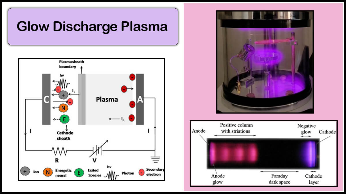
Vac Coat vacuum coaters for electron microscopy are able to perform deposition of metal and carbon thin films to enhance electrical conductivity of the sample’s surface, produce bio-sample’s replica, coating TEM grids, and improve their hydrophilicity. Vac Coat vacuum coating systems and SEM coaters, including low and high vacuum SEM coaters, DSR1 and DST1, low and high vacuum carbon coater, DCR and DCT, and hybrid coaters, such as DSCR, DSCT, and DSCT-T, with optional glow discharge plasma treatment ability are ideal coating devices for electron microscope sample preparation.
Some Of Vac Coat's Products


References
- Wu, J., Shaw, C. M., & Martin, D. C. (2012). Electron microscopy of organic materials: an overview and review of recent developments.
- https://www.mri.psu.edu/materials-characterization-lab/characterization-techniques/transmission-electron-microscopy#:~:text=In%20a%20transmission%20electron%20microscopy,sensitive%20or%20low%20contrast%20samples
- https://ares.jsc.nasa.gov/research/laboratories/transmission-electron-microscopy.html#:~:text=In%20a%20transmission%20electron%20microscope,Mars%2C%20comets%2C%20and%20asteroids
- Moradifar, Parivash, et al. “Accelerating quantum materials development with advances in transmission electron microscopy.” Chemical Reviews 123.23 (2023): 12757-12794.
- Koster, A. J., et al. “Three-dimensional transmission electron microscopy: a novel imaging and characterization technique with nanometer scale resolution for materials science.” The Journal of Physical Chemistry B 104.40 (2000): 9368-9370.
- https://www.nanoscience.com/techniques/transmission-electron-microscopy/
- https://en.wikipedia.org/wiki/Annular_dark-field_imaging
- https://www.sciencedirect.com/topics/physics-and-astronomy/transmission-electron-microscopy
- https://myscope.training/TEM_practicalTab
- https://pmc.ncbi.nlm.nih.gov/articles/PMC3907272/
- https://www.otago.ac.nz/omni/electron-microscopy/tem-techniques
- https://www.azolifesciences.com/article/TEM-Imaging-Modes.aspx
- https://en.wikipedia.org/wiki/High-resolution_transmission_electron_microscopy