Thickness Control of Carbon Film in Vacuum Carbon Coaters
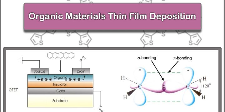
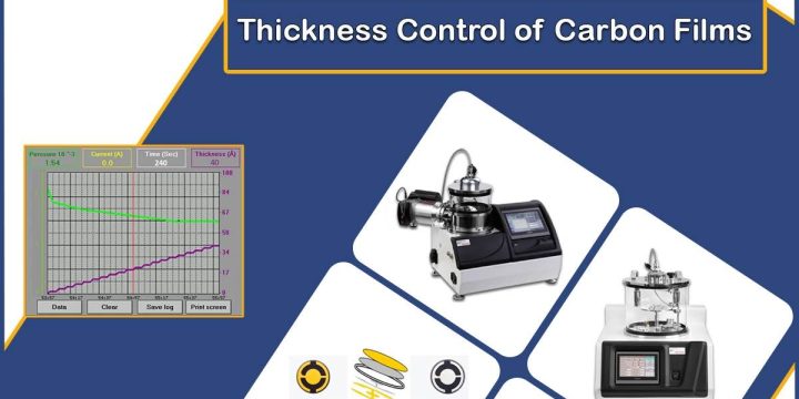
[vc_row][vc_column width="3/4"][vc_row_inner][vc_column_inner width="1/2"][vc_column_text css=""] Precise Thickness Control of Carbon Film in Vacuum Carbon Coaters Control of carbon film thickness deposited on the samples to be analyzed by electron microscopy (SEM, TEM, FE-SEM, and etc.) or Energy-dispersive X-ray spectroscopy (EDX) should be accurate to obtain the best result. The QCM monitoring of the thickness of carbon thin film deposition by resistive evaporation of carbon sources (Rod or Fiber) happens at high temperatures that may cause sensor heating and failure. [/vc_column_text][/vc_column_inner][vc_column_inner width="1/2"][vc_column_text css=""] [lwptoc backgroundColor="#d6d6d6" borderColor="#5b5b5b" skipHeadingText="Recent Posts|Some of Vac Coat Products|Sputter Coater|Carbon Coater|SEM Coater|Thermal"] [/vc_column_text][/vc_column_inner][/vc_row_inner][vc_row_inner css=".vc_custom_1736513625084{background-color: #D9D9D9 !important;}"][vc_column_inner width="1/2"][vc_cta h2="" txt_align="center" style="3d" color="mulled-wine" add_button="bottom" btn_title="What is SEM?" btn_style="3d" btn_color="juicy-pink" btn_align="center" btn_link="url:https%3A%2F%2Fvaccoat.com%2Fblog%2Fscanning-electron-microscope-sem%2F|title:Scanning%20Electron%20Microscope%20(SEM)|target:_blank"][/vc_cta][/vc_column_inner][vc_column_inner width="1/2"][vc_cta h2="" txt_align="center" style="3d" color="mulled-wine" add_button="bottom" btn_title="Carbon Coaters" btn_style="3d" btn_color="juicy-pink" btn_align="center" btn_link="url:https%3A%2F%2Fvaccoat.com%2Fcarbon-coater%2F|title:Carbon%20Coaters%20%7C%20Vac%20Coat%20Desk%20Carbon%20Coaters|target:_blank"][/vc_cta][/vc_column_inner][/vc_row_inner][vc_row_inner][vc_column_inner width="1/2"][vc_column_text css=""] Pulsed Carbon Fiber Evaporation Process Pulsed…