Energy-Dispersive X-Ray Spectroscopy
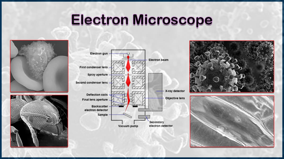
Energy-dispersive X-ray Spectroscopy (EDXS) is a useful analytical technique for the detection of the elemental composition of a sample, typically executed along with electron microscopy imaging (SEM or TEM). This X-ray microanalysis method that is also called Energy-dispersive Spectroscopy (EDS), empowers qualitative and quantitative mapping of the elements existing in a thin film which is useful in product research and deformulation.
Elemental Analysis of Materials in Electron Microscopy
There are three methods to identify the elements in a specimen while using electron microscopy:
- Energy-Dispersive X-Ray Spectroscopy (EDS/EDX), analyzing x-ray emission energy from the material after electron/x-ray beam interaction with it.
- Wavelength Dispersive Spectroscopy (WDS), which is the spectroscopic counterpart of EDS differs in using the diffraction of X-rays on special crystals to separate the acquired data into wavelengths. WDS with a much finer spectral resolution compared to EDS, avoids the problems, like false peaks and noises, in EDX.
- Electron Energy-Loss Spectroscopy (EELS), detects the energy distribution of the electrons after inelastic interaction with the material. EELS is a more difficult technique but works better at relatively low atomic numbers with higher energy resolution, compared to EDX.
Principles of Energy-Dispersive X-Ray Spectroscopy
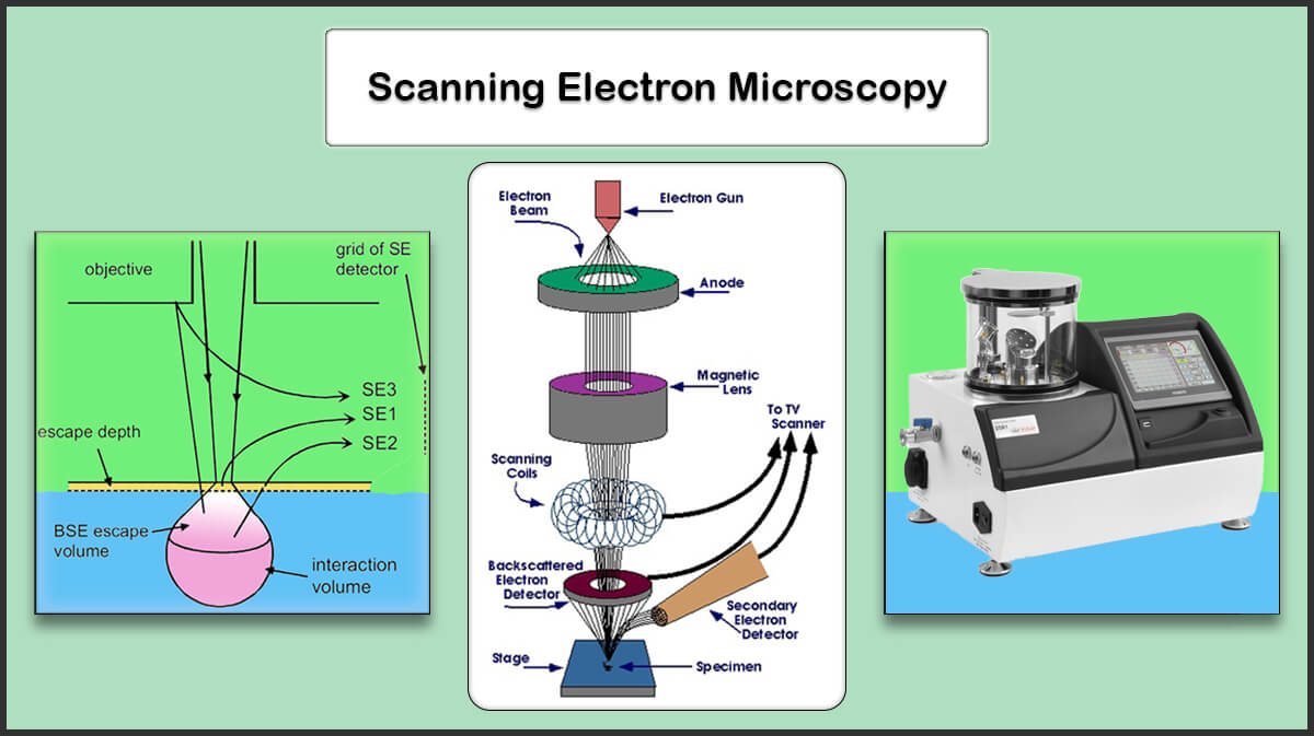
In the energy-dispersive X-ray spectroscopy technique, a beam of accelerated electrons (Or X-ray) is focused into the specimen under study to stimulate the emission of characteristic X-ray peaks from it (Figure 1). Each element in the periodic table has its own characteristic peak sets in the X-ray region, which are used to determine its existence in the sample.
X-Ray Generation from the Sample
When a sample is bombarded with a beam of high-energy electrons, elastic or inelastic electron-atom collisions can occur. Inelastic scattering of incident electrons from the bounded electrons or the nucleus of the atoms in the material, results in the production of two types of X-rays: Bremsstrahlung X-rays and Characteristic X-rays.

- Bremsstrahlung –braking radiation– X-Rays are created by deceleration of the incident beam electrons by the electric field around the nuclei of the atoms in the sample, where the lost energy is emitted as a continuum X-ray radiation, with energies not exceeding the energy of the primary electron beam.
- Characteristic X-Rays are produced by excitations of atoms from their ground state of energy. Since the atoms are willing to return to their ground state, they emit the absorbed energy in the form of photons that lay in the X-ray region.
Characteristic X-Ray Peaks
The atoms of each element contain a nucleus made up of neutral neutrons and positively charged protons (The number of protons defines the atomic number Z), and negatively charged electrons reside in orbitals (Shells) surrounding the nucleus named K, L, M, etc., as described by quantum mechanics. The electrons in each shell have specific ionization energies that are different for every element.
Characteristic X-rays are created by electron transitions between the inner electron shells. Initially, an electron from the inner shell absorbs the energy of the incident electron beam and is excited to a higher energy level (Shell), which is an unstable state. Then, the inner shell vacancy is filled with an electron from an outer shell, emitting an X-ray photon with an energy equal to the energy difference of the two shells, so the atom returns to a more stable state (Figure 2).

EDX Spectrum and Elemental Mapping
The X-ray microanalysis is based on the specific ionization energies of each shell (And subshells) for each element, which leads to distinctive energy of the produced X-ray photon that is a characteristic of the element under study. For example in the Si atom, the ionization energy of the K and L shells are 1.84 keV and 0.10 keV, respectively. Recording the number of X-ray characteristic photons from each element gathered from every point during a fixed counting time can create an elemental X-ray map from the specimen (Figure 3).

EDS vs WDS
The characteristic X-ray lines can be detected utilizing an energy dispersive detector (Usually a semiconductor detector) in EDS analysis or go through a diffracting crystal to separate different wavelengths in a wavelength dispersive spectroscopy (WDS), so each energy peak is converted into its wavelength counterpart. Hence, EDS and WDS characterization methods differ mainly in the detection and analyzing procedure.


Figure 3. Schematic of An Electron Microprobe with WDS Analyzer (Left) and Spectrum Resolution in EDS and WDS (Right).
Consequently, WDS is ideal for resolving closely spaced X-ray lines and distinguishing between elements with overlapping X-ray emissions with 10 times better resolution compared to EDS, no need to peak deconvolution. Also WDS can help to analyze trace elements below the detection limits of EDS.

Parts of Energy-Dispersive X-Ray Spectrometer
All EDX spectrometers are composed of four main parts:
- Excitation source (Electron or x-ray beam), as used in SEM/STEM or XRF systems
- Detector, to convert x-ray energy into voltage signals
- Pulse processor, to measure the signals
- Multi-channel analyzer, to display the data
EDX spectrum difference in SEM and TEM
The basic principle of EDX analysis is the same in SEM and TEM imaging, although, according to the different structures and operating accelerating voltages of the two types of microscope, there are some differences in EDS detector performance.
Accelerating Voltage. In EDX analysis during SEM imaging, an accelerating voltage of about 30 kV should be used to ensure efficient X-ray generation. However, higher accelerating voltages that are used in TEM imaging, can emerge higher energy X-ray photons related to K and L lines for elemental identification.
Spatial Resolution. The spatial resolution in EDX analysis strongly depends on the interaction volume of the incident electron beam, which is affected by the accelerating voltage and the sample atomic number (Z). The spatial resolution and depth resolution of EDS in the SEM is about a few microns, while in the TEM imaging higher energy electron beam is utilized to penetrate thin foils of the specimen, which leads to a better spatial resolution on the order of sample thickness, typically about 10-200 nanometers.
Detection Limit. The detection limit of EDX analysis is in the range of 0.1-0.5 wt% in the SEM and depends on the composition of the sample, but misses the sensitivity for analysis of trace elements. However, detection limits of approximately 0.01-0.1 wt% can be achieved in the TEM.
Sample Preparation For The EDX Analysis
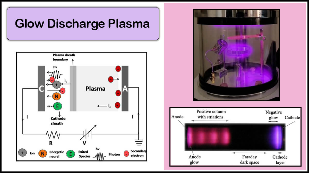
Conventional sample preparation procedure for qualitative Energy-dispersive X-ray spectroscopy may include several steps, nearly the same as the sample preparation for the SEM/TEM, as sectioning, polishing (A polished and flat surface is recommended in EDX analysis), dehydration, fixation, plasma treatment for removing contaminations and coating with a thin film of suitable material, like metals or carbon, to make the sample conductive (In case of imaging non-conductive specimen).
Besides, biological samples go through extensive preparation before EDX analysis, which introduces interrupting X-ray artifacts into the results.
Coating EDX Samples
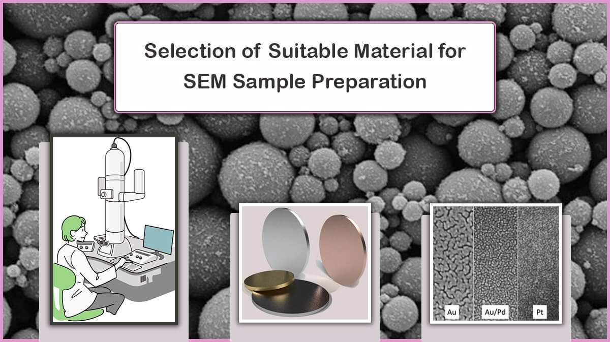
Charging the sample surface by the incident beam electrons during electron microscopy and EDX analysis can affect primary electron energies. To avoid surface charge accumulation, coating the sample with a precise selection of the material and thickness for coating the samples is a crucial step. However, the chemical nature of the coating material should be considered carefully to prevent the overlap of the resulting characteristic X-ray peaks from the sample and the coating layer.
Coating Thickness
A thin film with sufficient thickness to solve the charging problem may attenuate the incident electron beam energy and absorb the emitted X-ray photons. So the best coating on a sample for EDX analysis is the thinnest one to minimize the primary electron beam energy loss and X-ray adsorption within the sample and maximize the yield of x-ray flux. Also, thinner coating leads to smaller excitation of x-rays from the coating material. If thin films of carbon, aluminum, gold, and gold-palladium with a thickness of 5-10 nm are coated on the sample, the energy loss of the incident electron beam does not intensely affect the result.
Coating Materials Parameters
The selection of suitable material for coating the sample for EDX analysis has to be carefully considered due to several parameters, such as mass attenuation coefficient and interference of background and characteristic X-ray from the coating material and the sample.
Mass Attenuation Coefficients
Mass attenuation coefficient, i.e. absorption coefficient, for X-ray lines, is one of the key parameters to be noticed. This coefficient for X-ray lines from 0.5 to 1.5 keV is different for each element. Among the coating materials for EDX analysis, aluminum owns the lowest X-ray mass attenuation coefficient, followed in order by carbon, gold, and gold/palladium. In the region above 1.5 keV, the carbon attenuation coefficient is lower than Al, Au, and Au/Pd. However, from the viewpoint of electrical and thermal conductivity, Au is the best, with aluminum and carbon in the next ranks. It appears that aluminum is ideal for use with x-ray lines of 0.8-4 nm due to its physical properties, while carbon is preferable outside this zone.
Interference of Coating and Sample X-Ray Lines
The L and M X-ray characteristic lines of heavy metals like Au, Pd, Pt, etc., may overlap with the K lines of the light elements in the specimen.
Background X-Ray Radiation
The X-ray emission from the coating material can contribute to the X-ray spectrum background that may deteriorate the accuracy of quantitative EDX analysis relying on the background radiations.
Choice of Coating Material for Energy-Dispersive X-Ray Spectroscopy
Gold and Gold/Palladium coatings are typically used in sample preparation for electron microscopy to enhance secondary electron emission and better EM imaging, however, their characteristic and continuum x-ray radiation overlap with the X-ray lines of a small or trace amount of the interest materials in case of EDS analysis. Also, in the case of a specimen consisting of elements with a Z number greater than 10, the interaction of the coating with the beam and backscattered electrons obtained from the sample can excite unwanted radiation from the coating.
Four elements, beryllium, carbon, aluminum, and chromium are proved to be proper candidates as coating materials regarding quantitative analytical studies. The important properties of these materials and their advantages and disadvantages are discussed below.
Beryllium with low evaporation temperature, medium thermal and electrical properties, negligible x-ray interference, and minor contribution to background is a suitable material. However secure procedures and precautions should be employed to avoid its toxicity.
Carbon is the most common coating material and a thin layer of carbon appears to diminish charging in bulk samples. Easy application and little effect on the x-ray yield from the sample are advantageous features of carbon coatings. It should be noted that rather poor electrical properties of carbon films can be improved using high vacuum carbon coaters like DCT and DCT-300, as discussed in our blog article, effect of chamber ultimate pressure on carbon coating. However, the high evaporation temperature of carbon can easily cause thermal damage to the sample. Carbon coating has been widely used to coat frozen-dried sections and to provide a thin conducting layer to support such specimens.
Aluminum has low evaporation temperature, good electrical properties, and low adsorption coefficient, but is not suitable for coating light element materials, due to peak overlaps and contribution to the general background in x-ray microanalysis. Aluminum has been widely used in coating the support plastic films for the sections.
Chromium with satisfactory thermal and electrical properties to prevent specimen charging and avoid beam-induced thermal damage, and low evaporation temperature prevents thermal damage to the sample surface. In the case of biological samples, chromium characteristic X-ray lines are far away enough from the characteristic lines of the sample elements, so they do not hinder the identification procedure. However, the higher density of Cr coating enhances beam attenuation and absorption of soft X-rays emitted from samples, especially ones consisting of low-atomic-number elements, which is a serious drawback.

Coating Techniques
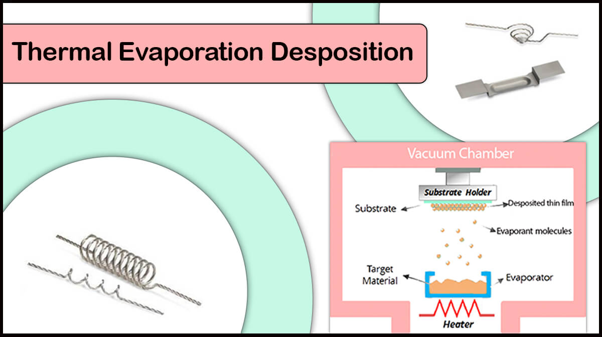
The coating workflow for the mentioned elements is relatively easy to perform, considering safety precautions in working with beryllium. All four materials are recommended to be coated using physical vapor deposition (PVD) techniques like thermal evaporation at high vacuum with standard sample rotation or planetary sample rotation to ensure a smooth coating on even rough surfaces. All Vac Coat SEM coaters are supplied with a sample rotation stage and an optional planetary rotating sample stage to obtain a uniform coating on the samples.
Limitations of Energy-Dispersive Spectroscopy
There are some limitations due to quantitative EDS analysis that are listed below:
- Hydrogen and Helium atoms with atomic numbers (Z) 1 and 2, respectively, do not have characteristic X-rays, so cannot be detected with the EDS technique
- The X-rays generated from K shell transitions in Li (Z = 3) atom have too low energy to be detected by EDS
- There exist problems in detecting EDS X-rays from Be (Z = 4) to Ne (Z = 10)
- Absorption of low energy X-rays passing through the specimen
- The detected X-ray peaks’ shape and position may change in different compounds since the same valence electrons that are involved in the chemical bonding of the element also generate the characteristic X-ray peaks
- Comprehensive analysis of samples containing structurally bound water or carbonate cannot be obtained through EDS
- EDS analysis does not provide information on the valence state of the oxygen-bonded cations to calculate oxygen by stoichiometry
- As mentioned previously, a thin film of carbon is commonly coated on non-conductive samples. So carbon-containing materials cannot be analyzed with EDX if coated with carbon and a different coating material must be chosen
Vac Coat SEM Coaters and EDX
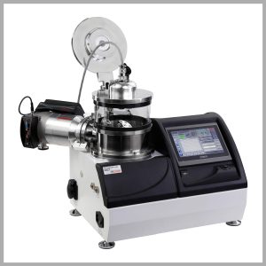
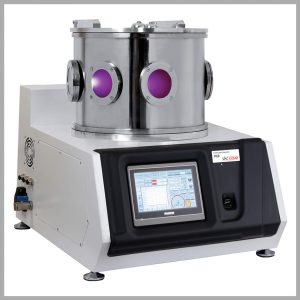
Vac Coat offers a variety of SEM coaters like magnetron sputter coaters (DSR1 and DST1), carbon coaters (DCR and DCT), and thermal evaporators (DTE and DTT), working at low or high vacuum conditions.
Multiple coating techniques are made available in Vac Coat hybrid coaters like DSCR, DSCT, and DSCT-T.
Vac Coat also manufactures large coating systems for research purposes like triple-target sputter coater (DST3) and combined double-target sputter coater with a thermal evaporator (DST2-TG) that enables co-deposition inclusively.
Vac Coat also offers various optional features like RF sputtering, substrate bias voltage, heater, and glow discharge plasma, which is applicable for plasma treatment and cleaning.
Some of Vac Coat Systems
References
- Pirozzi, Nicole M., Jeroen Kuipers, and Ben NG Giepmans. “Sample preparation for energy dispersive X-ray imaging of biological tissues.” Methods in Cell Biology. Vol. 162. Academic Press, 2021. 89-114.
- https://en.wikipedia.org/wiki/Energy-dispersive_X-ray_spectroscopy
- Goldstein, J. I., Newbury, D. E., Echlin, P., Joy, D. C., Romig, A. D., Lyman, C. E., … & Lifshin, E. (1992). Coating and conductivity techniques for SEM and microanalysis. Scanning Electron Microscopy and X-Ray Microanalysis: A Text for Biologists, Materials Scientists, and Geologists, 671-740.
- https://www.intertek.com/analytical-laboratories/microscopy/edx/
- Scimeca, M., Bischetti, S., Lamsira, H. K., Bonfiglio, R., & Bonanno, E. (2018). Energy Dispersive X-ray (EDX) microanalysis: A powerful tool in biomedical research and diagnosis. European journal of histochemistry: EJH, 62(1).
- https://myscope.training/pdf/MyScope_EDS.pdf
- https://ywcmatsci.yale.edu/facilities/sem/sample-preparation
- Walck, S. (2013). Sample preparation considerations for X-ray EDS analysis in the physical sciences. Microscopy and Microanalysis, 19(S2), 2012-2013.
- https://www.oxinst.com/blogs/difference-between-eds-and-wds-what-is-it-all-about
- https://rockymountainlabs.com/eds-and-wds-spectroscopy/
- https://www.mcswiggen.com/TechNotes/WDSvsEDS.htm

