Physical Vapor Deposition Market
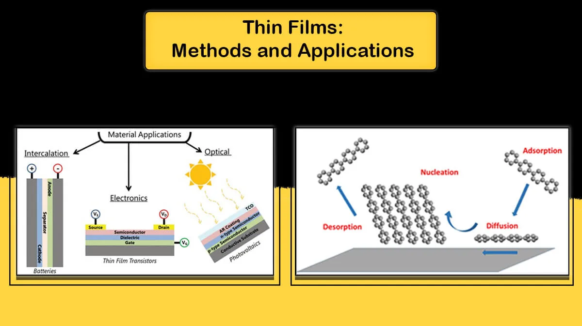
Physical Vapor Deposition (PVD) represents a cornerstone suite of techniques for depositing thin films of various materials onto substrates, operating under low or high vacuum conditions. Its versatility in handling a wide array of materials (Metals, alloys, ceramics, compounds) and its ability to tailor film properties (Thickness, adhesion, density, stress, electrical and optical characteristics) make it indispensable across numerous high-technology sectors.
As we look towards the next decade (2025-2035), PVD market trend is poised for significant growth and technological evolution, driven by relentless innovation cycles in its primary end-use markets. This analysis synthesizes data from recent market reports to provide a comprehensive outlook on the PVD landscape, highlighting key growth drivers, technological advancements, market segmentation, regional dynamics, and strategic considerations relevant from our current perspective in April 2025.
What is PVD Process?
PVD is a vacuum deposition process where material transitions from condensed to vapor phases before forming a thin film on a substrate. Primary PVD techniques include:
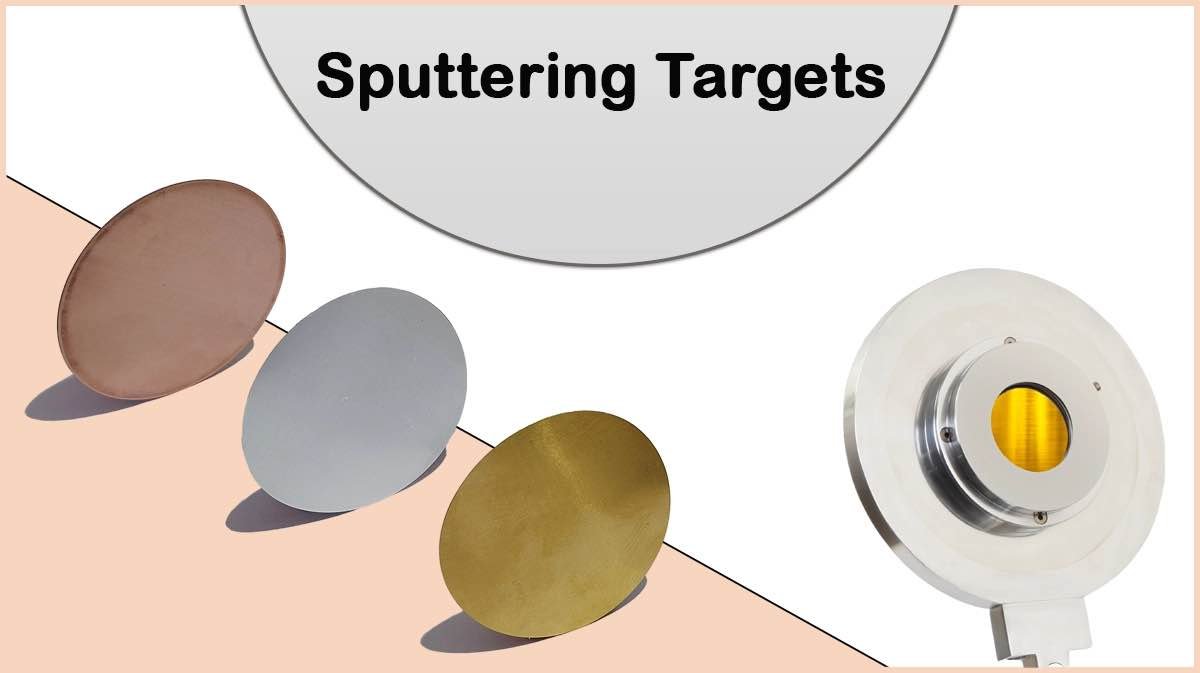
- Sputtering Deposition – Atoms are ejected from a target material due to ion bombardment and deposited onto a substrate
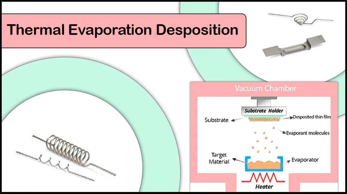
- Evaporation Deposition – Material is heated until it vaporizes and condenses on a substrate
- Arc Vapor Deposition – Uses electrical arcs to vaporize cathodic material, which then deposits as a coating
Global PVD Market: Size, Growth, and Structure
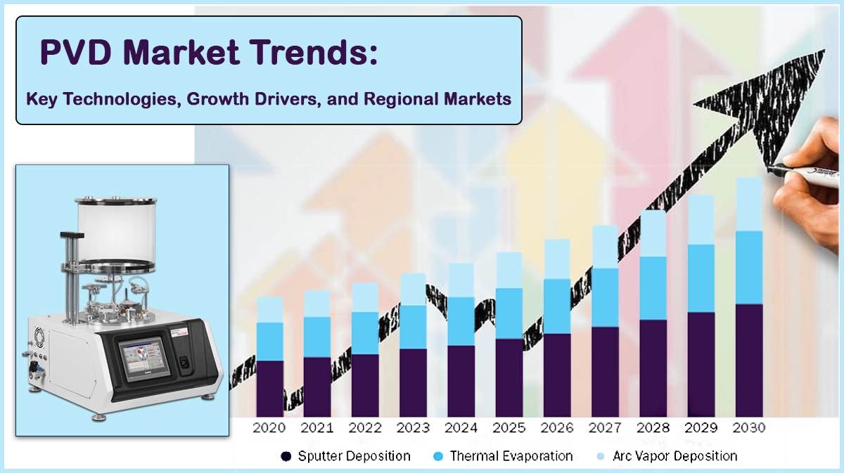
The global PVD market (Encompassing equipment, materials, and services) constitutes a substantial and rapidly expanding segment of the advanced manufacturing landscape. Recent analyses underscore this dynamism. For instance, a report highlighted by GlobeNewswire (Attributed to The Business Research Company) projects the global physical vapor deposition market to reach approximately $49.2 billion by 2033, indicating robust expansion from current levels (Figure 1). This report also noted a strong recent compound annual growth rate (CAGR) approximating 8.25%. While specific CAGR projections for the full 2025-2035 period can vary slightly between market research firms (Often falling within a 6% to 9% range in various reports), the consensus points towards sustained, significant growth exceeding that of the broader global economy.

Key Market Drivers Propelling PVD Growth (2025-2035)
The strong projected growth trajectory in PVD coating market is underpinned by powerful, long-term trends across several key industries:
✔ Microelectronics and Semiconductors – Rising demand for advanced node ICs (≤3nm), MEMS, and power electronics which can be satisfied through physical vapor deposition of ultra-thin, highly conformal, and defect-free barrier layers (e.g., Tantalum Nitride – TaN, Titanium Nitride – TiN), seed layers (Copper – Cu, Cobalt – Co), and potentially new interconnect metals (Like Ruthenium – Ru) or metal caps become exponentially more challenging.
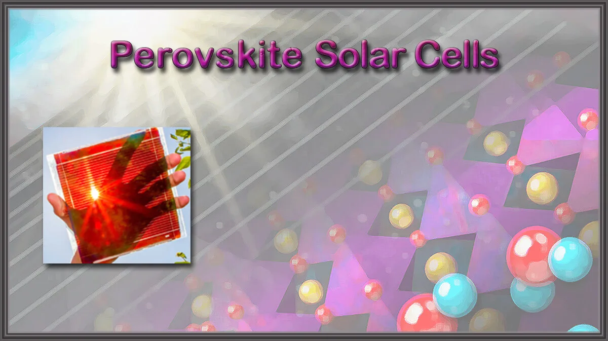
✔ Green Energy Sector – Thin-film PVD in solar cells for deposition of absorber layers in thin-film solar cells (Like CIGS – Copper Indium Gallium Selenide, and CdTe – Cadmium Telluride), metal contacts (Silver and Aluminum), and transparent conductive oxides (TCOs). Also, coating current collectors (Copper and Aluminum) in batteries as well as PVD applications in hydrogen fuel cells is gaining traction.
✔ Medical Applications – Need for biocompatible, antimicrobial, and wear-resistant coatings, can be achieved by PVD coating of biocompatible thin films of (TiN, ZrN, DLC) for implants (Orthopedic and dental) and surgical instruments, reducing friction, wear, and adverse biological reactions. It’s also used for conductive tracks and barrier layers in implantable electronic devices.
✔ Wear-Resistant Coatings in Industry, EVs (Electronic Vehicle), and Aerospace – Deposition of hard coatings (TiN, TiAlN, AlCrN, TiSiN, Diamond-Like Carbon – DLC) for cutting tools and wear parts, engine and powertrain components, and PVD coatings with thermal barrier properties, wear resistance, and corrosion protection for critical engine components and airframe parts operating in extreme environments.
✔ Optical Components – PVD helps in deposition of Anti-reflective coatings, high-reflectivity mirrors, TCOs (Like Indium Tin Oxide – ITO) for touch screens and pixel electrodes, metal layers for circuitry in TFT backplanes (LCD, OLED), etc.

Technology Segmentation and Key PVD Market Trends (2025-2035)
Within the physical vapor deposition market, different techniques satisfy varying needs, and significant evolution is underway:
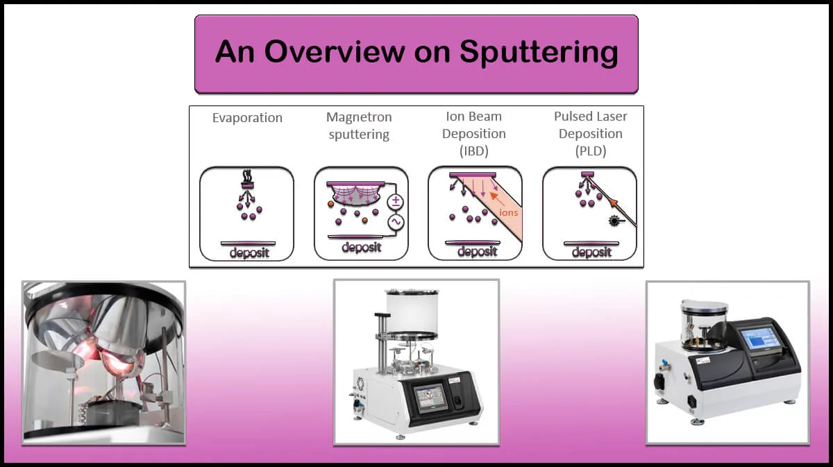
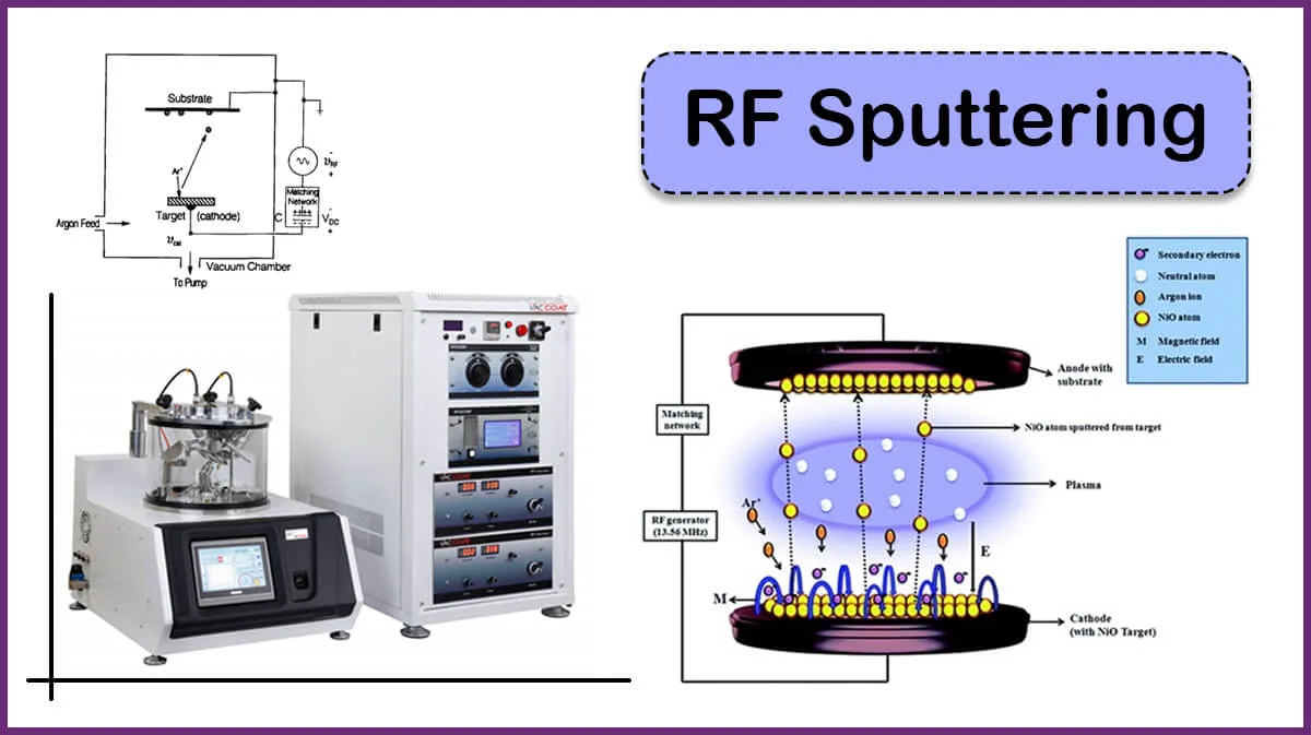
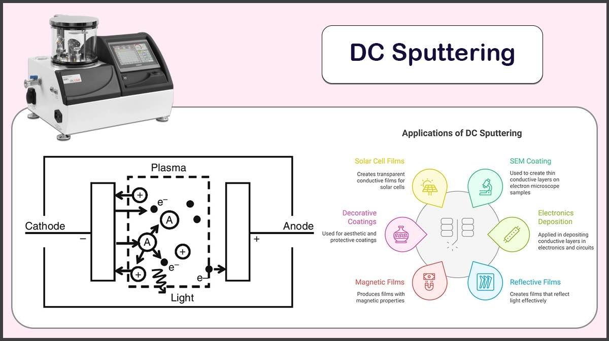
Sputtering
This remains the most widely used PVD technique due to its versatility, control over film composition (Especially with alloys and compounds via reactive sputtering), and ability to deposit a vast range of materials.
- Magnetron Sputtering (DC, RF, Pulsed DC): The workhorse for depositing metals and conductive materials (DC) and dielectric materials (RF or pulsed DC). Continuous improvements focus on target utilization, deposition rate, and film uniformity over large areas.
- High-Power Impulse Magnetron Sputtering (HiPIMS/HPPMS): This technique, characterized by short, high-power pulses, generates highly ionized plasma.

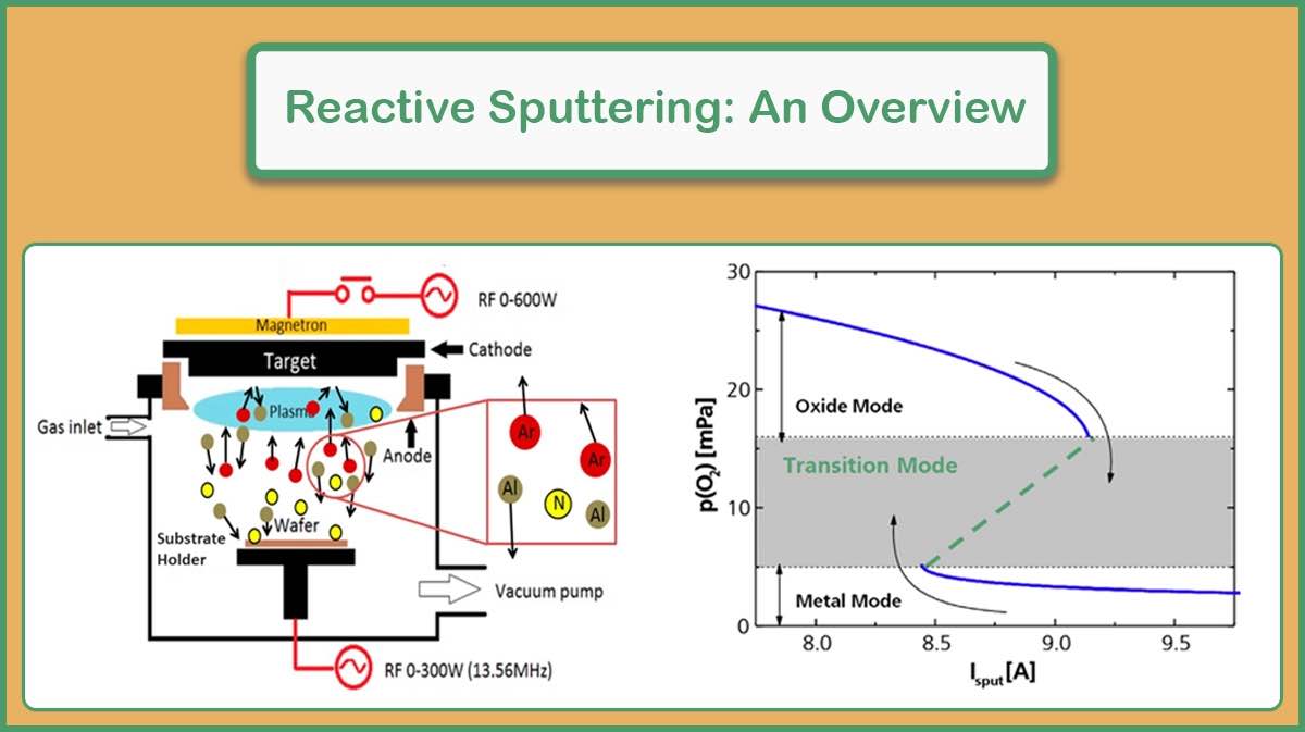
- Reactive Sputtering: Sputtering a metal target in the presence of a reactive gas (Like oxygen or nitrogen) to form oxides or nitrides is critical but challenging to control precisely. Advancements focus on sophisticated feedback loops (Monitoring plasma emission, voltage, or using lambda sensors) to maintain stable stoichiometry and avoid target poisoning, enabling high-quality deposition of materials like ITO, AlN, SiO2, TiO2, SiN, etc.
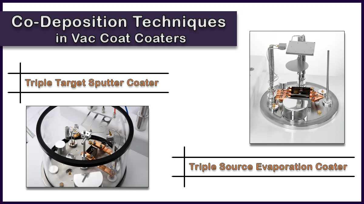
- Co-Sputtering: Using multiple sputtering sources simultaneously allows for the deposition of alloy films with tailored compositions or functionally graded materials. This is increasingly important for developing new materials with specific electrical, mechanical, or optical properties (e.g., AlScN, phase-change memory materials, advanced barriers).
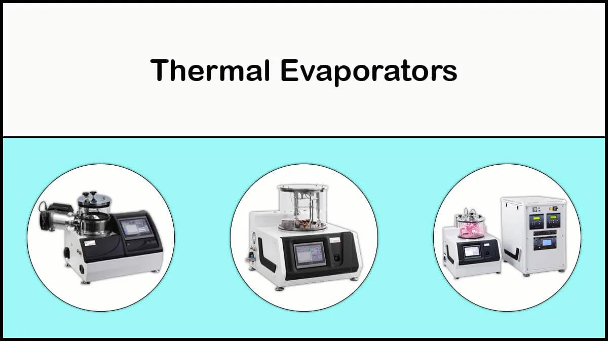
Evaporation
While generally simpler and sometimes cheaper than sputtering, evaporation (Including thermal and electron-beam methods) offers high deposition rates for certain materials and is preferred for applications sensitive to plasma damage or requiring high purity lift-off processes (Common in some compound semiconductor applications). It remains important for optical coatings, some metal layers in electronics, and decorative coatings. However, it typically offers poorer step coverage and less control over film structure compared to advanced sputtering techniques.

Cross-Cutting Technological PVD Coating Market
- Material Evolution: Demand for depositing new and complex materials, including high-entropy alloys, complex oxides, nanolaminates, and materials for emerging computing paradigms (Neuromorphic and quantum interfaces).
- Precision and Control: Ever-tighter specifications require enhanced control over film thickness uniformity (Sub-nanometer scale), stress, stoichiometry, grain structure, and defect density across larger substrate sizes (e.g., 300mm wafers, large glass panels).
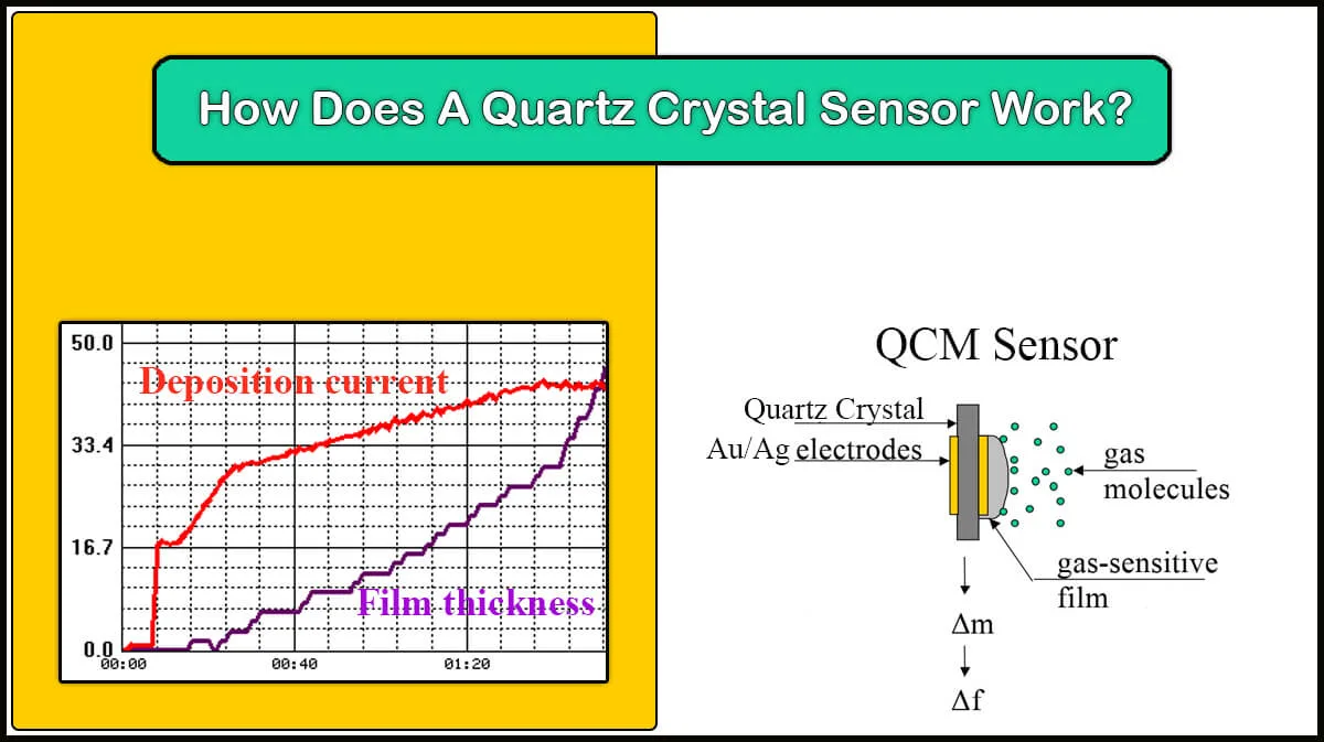
- In-Situ Metrology and Process Control: Integration of real-time monitoring techniques (Optical Emission Spectroscopy – OES, mass spectrometry, quartz crystal microbalances (QCM), ellipsometry) directly into PVD chambers, coupled with advanced feedback control algorithms (Potentially leveraging AI/ML), is becoming crucial for yield improvement and process stability, especially for complex reactive sputtering or HiPIMS processes.

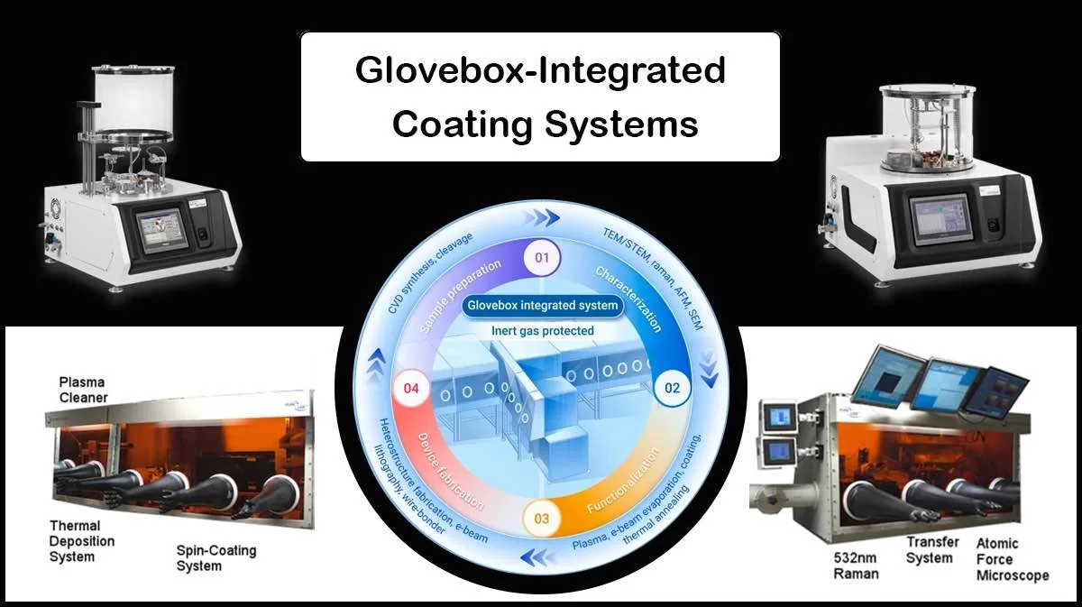
- Cluster Tools and Glovebox Integration: PVD modules are increasingly integrated into large vacuum cluster systems, including gloveboxes, that combine multiple process steps (e.g., pre-clean/etch, PVD, CVD, ALD, anneal) without breaking vacuum. This is essential for advanced semiconductor manufacturing to avoid contamination and enable complex device structures. Hybrid PVD/ALD processes are also emerging for specific applications requiring a combination of PVD’s speed and ALD’s conformity.
- Multi-Target Sputtering: Enables complex alloy and composite coatings for next-gen EVs and solar cells.
- Sustainability: Increasing focus on improving target material utilization (Reducing waste), enhancing energy efficiency of plasma sources and vacuum systems, and exploring alternatives to potentially hazardous materials where feasible.
Regional PVD Market
The global PVD market exhibits distinct regional characteristics:
- Asia-Pacific (APAC): This region stands as the largest and fastest-growing PVD market with over 40% of the market share (At 2024), driven by its dominance in
- Semiconductor manufacturing (Taiwan, South Korea, China, Japan)
- Display production (South Korea, China)
- Solar cell manufacturing (China, India), which fuels demand for high-efficiency thin-film coatings
- General electronics assembly: Massive investments in fab construction and government initiatives supporting domestic high-tech industries fuel this leadership.
Result in a CAGR: 6.7% (2024-2034), driven by government-backed R&D.

- North America – High Growth Market: A major PVD market size with significant strength in advanced semiconductor R&D and manufacturing in aerospace, defense, and cutting-edge research
- Semiconductor re-shoring (Intel, TSMC Arizona) boosts local PVD demand
- Medical device coatings (U.S. leads in surgical tools and implants)
- EV & Aerospace industries seek advanced wear-resistant PVD coatings
- Europe – Sustainability Focused: Holds a strong position in automotive manufacturing, industrial equipment, high-end tooling, medical technology, and research and development.
- Stringent environmental policies promote low-toxic and energy-efficient PVD techniques
- Growth in automotive (Germany), aerospace (France), and medical applications
- EU Chips Act aims to significantly strengthen Europe’s semiconductor ecosystem
Competition and Strategy in PVD Equipment Market
Applied Materials is frequently cited as the PVD market leader, particularly strong in the semiconductor equipment segment. Other major global players consistently identified across reports include OC Oerlikon (Specifically its Surface Solutions segment), Lam Research, ULVAC Technologies, Buhler Leybold Optics, Von Ardenne, Evatec, Kobe Steel, Veeco Instruments, and IHI Hauzer Techno Coating.
These companies mostly invest heavily in R&D of PVD market trends and offer comprehensive PVD system portfolios, often integrated into larger platforms. However, the fragmented nature beyond these leaders allows specialized players to thrive by focusing on specific PVD technologies (e.g., HiPIMS specialists), application niches (e.g., optical coatings, large-area glass), or regional markets.
Strategic imperatives for companies involved in physical vapor deposition market (Equipment makers, material suppliers, end-users) over the next decade include:
- Continuous Technological Innovation: Developing next-generation PVD sources (Advanced HiPIMS, controlled reactive sputtering), improving uniformity and throughput, enabling deposition of new materials
- Application-Specific Solutions: Tailoring PVD systems and processes to meet the unique demands of high-growth sectors like advanced packaging, micro-LEDs, or specific medical coatings
- Cost-Effectiveness: Balancing advanced capabilities with competitive cost-of-ownership (Throughput, target utilization, and system uptime)
- Strategic Partnerships and Collaborations: Working across the value chain (Materials suppliers, equipment vendors, end-users, research institutes) to accelerate development and adoption
- Geopolitical Adaptation: Navigating global supply chain complexities and leveraging regional initiatives like the Chips Acts
- Service and Support: Providing robust global service infrastructure is critical for complex PVD equipment
Challenges and Future Outlook of PVD Market
Despite the strong growth of PVD coating market, the following challenges remain:
- High Equipment and Maintenance Costs: $500K–$3M per PVD system, limiting small-scale adoption
- Supply Chain Volatility: High-purity target materials like Titanium, Zirconium, Tantalum price fluctuations impact profitability
- Competition from ALD and CVD: ALD is growing in advanced semiconductor nodes (<5nm), while CVD remains dominant in solar
However, the fundamental need for precise, functional thin films across nearly every advanced technology sector ensures a bright future for PVD. Its adaptability and the ongoing innovation within PVD techniques themselves will allow it to meet evolving demands. The next decade will likely see PVD coating market become even more sophisticated, integrated, and essential to enabling next-generation electronic devices, energy solutions, and high-performance industrial products.
Physical Vapor Deposition Global Market Report
The PVD thin film deposition market is on a high-growth trajectory, driven by advancements in microelectronics and semiconductor scaling, green energy, and precision manufacturing. Strategic investments in new deposition techniques, eco-friendly coatings, and regional expansion will define PVD market leaders over the next decade.
The PVD market trends demand a focus on mastering advanced deposition techniques like HiPIMS and reactive sputtering, exploring novel material combinations through co-sputtering, and understanding the integration of PVD within complex device manufacturing flows. Expertise in plasma physics, material science, vacuum technology, and process control (Including data analytics/AI for optimization) will be paramount.
The sputtering process remains a vital component of the expanding PVD market, offering superior coating solutions for a wide range of applications. As industries continue to demand higher performance and precision, sputtering technology will play a crucial role in shaping the future of thin-film deposition. Stakeholders should focus on process optimization, cost reduction, and sustainable practices to capitalize on the growing opportunities in the physical vapor deposition market.
Vac Coat in PVD Equipment Market
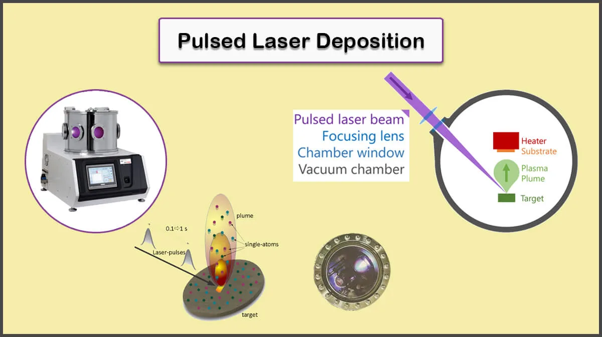
Vac Coat Company as a highly experienced manufacture of a wide range of PVD systems, such as magnetron sputtering systems, thermal evaporators, and pulsed laser deposition (PLD) devices, provides versatile coaters for hi-tech research projects.
Vac Coat deposition systems with thermal evaporation capability (DTE, DTT, DSCT, DST2-TG, and DST3-T) provides controlled deposition of wide range of evaporation sources with real-time thickness monitoring through QCM thickness meter.
Some of Vac Coat Systems


References
Physical Vapor Deposition Market Opportunities and Strategies to 2033.
- Physical Vapor Deposition Market Size, Share & Trends Analysis Report by Product (Sputter Deposition, Arc Vapor Deposition), By Application (Semiconductor & Electronics, Solar Products), By Region, And Segment Forecasts, 2024 – 2030.
- Vapor Deposition Market, By Process (CVD and PVD), By Application (Into Microelectronics, Cutting Tool, Medical Devices & Equipment and Decorative Coatings) and by End-Use (Electrical & Electronics, Automotive, Aerospace) – Forecast till 2032
Physical Vapor Deposition Market Size, Share, and Trends 2024 to 2034.
- Physical Vapor Deposition Market Outlook (2022 to 2032)
It’s encouraging to see continued investment and innovation in vacuum coating technologies. I wonder how much of the projected PVD market growth is being driven by sustainability goals or shifts in manufacturing priorities?
A significant portion of the projected PVD market growth over the next decade is directly tied to sustainability goals and manufacturing priorities alteration, which accounts for approximately 25–30% of the total market expansion, due to environmental regulations, renewable energy applications, increasing material efficiency, etc., according to insights drawn from the research reports mentioned in the text references.