
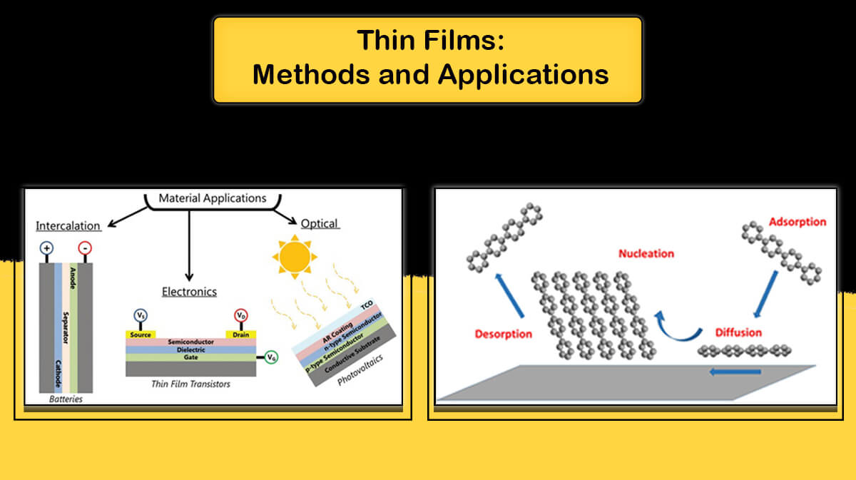
What Are Optoelectronics?
Optoelectronics include electronic components related to optics (light), in which the light is emitted, modified, or converted, and are activated or deactivated based on the intensity of light. These devices contain various parts like emitters and photodetectors, including photodiodes and phototransistors, which are significantly reliant on high-quality thin film deposition of metals and semiconductors.

Physical Vapour Deposition (PVD) method to create thin film coatings in optoelectronic devices is employed to deposit metals like aluminium or copper, as well as insulators such as silicon dioxide or nitride. The films created through this process are essential in the production of optoelectronic devices, acting as conductive paths, barriers, or insulators.
This adaptable method utilizes PVD techniques such as sputtering or evaporation to deposit materials on an atomic or molecular scale. What sets PVD thin film deposition in optoelectronics apart is its high purity and uniformity. These characteristics are critical for ensuring dependable semiconductor functionality. Nevertheless, it necessitates complex high vacuum conditions along with meticulous control. Its ability to scale up is a significant benefit for mass production. As the demand for smaller, faster, and more energy-efficient semiconductor devices rises, PVD thin film coatings in optoelectronic devices is becoming increasingly essential.
PVD Coating Processes in Optoelectronics
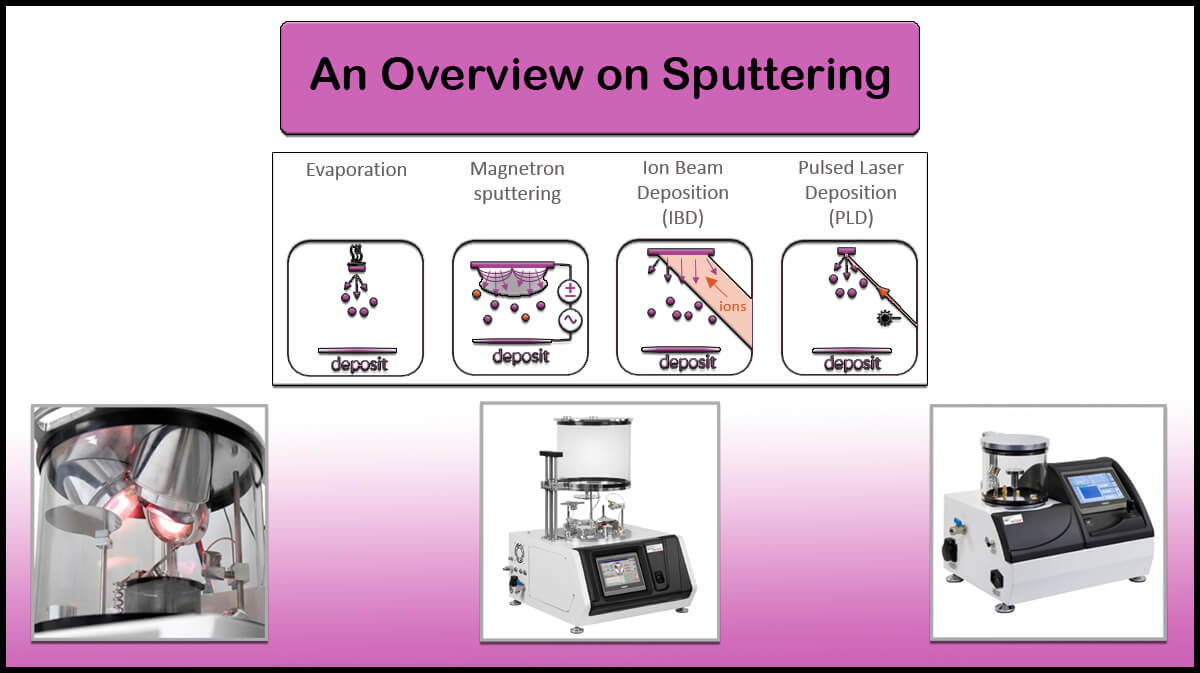
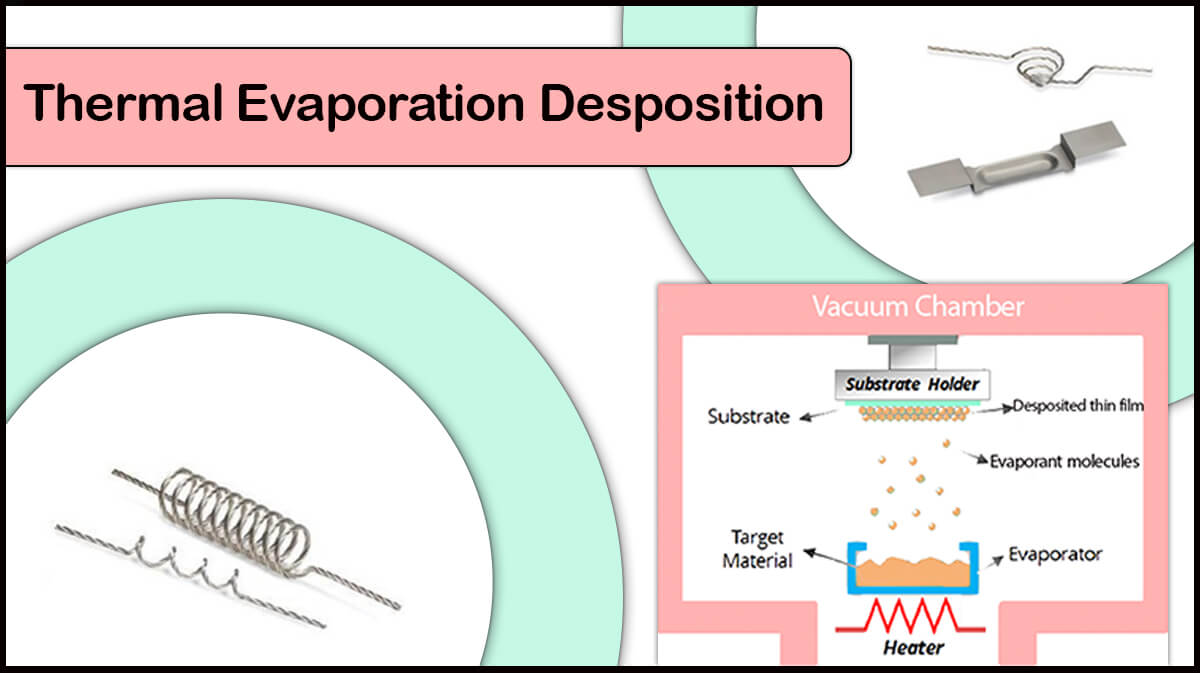
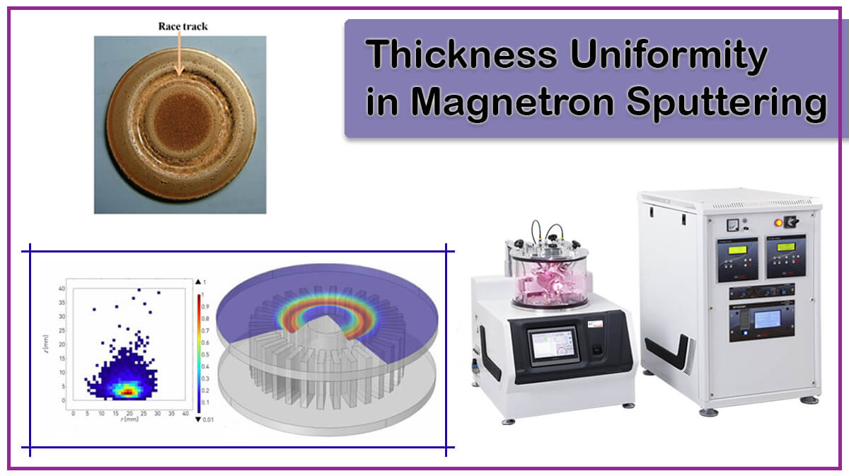
In the optoelectronic industry, there are two types of Physical Vapour Deposition (PVD) processes: sputtering and evaporation (Figure 2). Both procedures entail converting the source material into a vapour, which is subsequently delivered across a vacuum chamber to the substrate. However, they differ in how the source material is vaporised and the properties of the resultant film.
Cathodic arc PVD is a type of PVD process in which a source material is vaporised using a high-current electrical arc. This approach has significant benefits for semiconductor applications, notably in terms of corrosion protection.

Materials for Thin Film Coating in Optoelectronics
In the optoelectronic industries, PVD coating processes may deposit a wide range of materials. These materials have a variety of applications in optoelectronic device fabrication, including the formation of conductive layers, barriers, and insulating layers. The material used is determined by the film’s desired electrical, thermal, and mechanical qualities, as well as its compatibility with the underlying substrate and other materials in the device.
Metal Coatings
Metals are often utilised in PVD coating for semiconductors due to their high electrical conductivity and compatibility with different substrates. Aluminium, copper, gold, and silver are some of the most common metals utilised in semiconductor technology. These metals can be deposited as pure elements or alloys, depending on the desired film characteristics and device specifications.
Aluminium
Aluminium is commonly utilised in the production of interconnects and electrodes, since it provides an excellent blend of electrical conductivity, thermal stability, and cost-effectiveness. However, aluminium is sensitive to electromigration, which can eventually cause device failure.
Copper
Gold
Gold is used in applications that demand high electrical conductivity and oxidation resistance, such as wire bonding and ohmic contacts.
Silver
Silver, while less often utilised, can be used in a variety of applications where its high electrical conductivity and thermal stability are beneficial.
Chromium
Chromium is also a common material for PVD coatings because of its great hardness, superior corrosion resistance, and low coefficient of friction.

Ceramics
Ceramics are another type of material used in PVD coating of semiconductors. These materials are usually insulators or dielectrics, which means they don’t conduct electricity. Ceramics are used in a variety of applications within semiconductor devices, including insulating layers, dielectric barriers, and protective coatings. Silicon dioxide, silicon nitride, and aluminium oxide are some of the most prevalent ceramic materials utilized in PVD semiconductor coatings.
Silicon Dioxide
Silicon dioxide (SiO2) is a commonly used insulator in the optoelectronic industry. It functions as a gate dielectric in metal-oxide-semiconductor (MOS) devices, and an interlayer dielectric (ILD) between metallic interconnects. SiO2 exhibits outstanding electrical and thermal properties, including a high dielectric constant and low leakage current, making it an ideal material for these applications.
Silicon Nitride
Silicon nitride (Si3N4) acts as a barrier layer, preventing metals like copper from diffusing into the underlying silicon substrate. Si3N4 exhibits excellent thermal stability and barrier characteristics, which contribute to the device’s structural integrity and prevent performance degradation.
Aluminium Oxide
Aluminium oxide (Al2O3) is a ceramic substance utilised in PVD coatings due to its insulating qualities and chemical resistance. It can be applied as a protective coating on the surface of semiconductor devices, insulating them from external influences such as moisture and pollutants. Al2O3 also has a high dielectric constant, making it appropriate for use as a gate dielectric in certain advanced device topologies.
Coatings of such non-conductive materials can be performed through RF sputtering of the ceramic target. Vac Coat sputter coater with large chambers, like DST1-300, DSCR-300, DSCT-300, DST3, and DST2-TG can be equipped with RF power supply to enable sputter deposition of insulating materials.
Because if their low thermal conductivity, ceramic targets should be back-plated to prevent cracking. For more information, please visit https://vaccoat.com/blog/why-should-a-sputtering-target-be-back-plated/.


Organic Materials
Organic materials are also widely studied for use in optoelectronic devices, such as organic photovoltaic devices (OPVs), organic light-emitting diodes (OLEDs), and organic field-effect transistors (OFETs). The PVD coating techniques for the deposition process of such materials is based on the temperature-controlled thermal evaporation of the organic matters like polymers.
Deposition Process Parameters
The choice of source material, and the process parameters such as pressure, deposition rate, deposition temperature, and substrate temperature are all important in defining the final film qualities. Controlling the process parameters is crucial, especially when depositing ceramics, using PVD techniques to achieve the desired film qualities, including composition, thickness, and uniformity.
Film thickness, homogeneity, and substrate adhesion all have a substantial impact on semiconductor device performance and reliability. As a result, a thorough understanding of the PVD process and the characteristics of deposited materials is essential for successful deployment in the semiconductor sector.
Applications of PVD Coating in Optoelectronic Devices
PVD coating is important in the high-tech realm of optoelectronics since it helps to construct sophisticated gadgets. It serves as the foundation for thin-film transistors, which are key components in screens and LEDs. PVD generates low-resistance interconnects, which improve signal speed and device dependability. Furthermore, it protects semiconductors with protective coatings, assuring their longevity even in harsh situations.
From microchips to solar cells, PVD coating is the unsung hero that enables the next generation of optoelectronics. PVD coating has a wide range of applications in semiconductors, including microelectronics, optoelectronics, and power devices. PVD coating technique is also used in the manufacturing sector to make wear-resistant cutting tools. Coatings in micrometers (µm) enhance the durability and performance of solid materials, such as carbides.

Microelectronics
PVD coating is widely used in microelectronics for the fabrication of integrated circuits (ICs). These are miniature electrical circuits made up of several components, such as transistors, diodes, resistors, and capacitors, all integrated into a single chip. Metal layers are used to connect the components, and they are commonly deposited using PVD processes.

In all these applications, the management of PVD process parameters, such as temperature, pressure, and deposition rate, is crucial for achieving the desired film characteristics and optimal device performance. This necessitates a thorough understanding of the PVD process and the properties of the deposited materials, emphasising the importance of technical knowledge in this field.


Integrated Circuits (ICs)
Integrated Circuits (ICs) offer a prominent application area for PVD coating in the semiconductor sector. ICs are essentially miniature electronic circuits made of semiconductor material, typically silicon. IC manufacture comprises multiple phases, several of which use PVD methods to deposit various materials.
The production of the transistor, the fundamental building block of electronic devices, is an important milestone in integrated circuit fabrication. Metal-oxide-semiconductor (MOS) technology is commonly used in the fabrication of transistors in integrated circuits. In this method, a thin layer of silicon dioxide (SiO2) is deposited on the silicon substrate using PVD techniques to generate the transistor’s gate oxide. This layer acts as an insulator, allowing the gate to control the flow of current through the transistor while maintaining a direct electrical separation.
Another key stage in IC production where PVD is used is connection construction. These are conductive channels that connect the various components of the IC, allowing electrical impulses to pass across the device. Interconnects are often made of copper or aluminium, which are created utilising PVD processes like sputtering and evaporation. A barrier layer of coating material, such as titanium or tantalum, is frequently put before the metal layer to prevent diffusion between the metal and the underlying silicon.
In all these steps, controlling the PVD process parameters is crucial for achieving the desired film characteristics and performance. This encompasses the deposition rate, film thickness, and homogeneity, as well as the composition and purity of the deposited material. The ability to regulate these parameters accurately is one of the reasons why PVD is a popular technology for material deposition in IC production.
Advantages of PVD Coating in Optoelectronics
PVD coating offers various advantages in optoelectronic and semiconductor applications, with distinct benefits and applications in each discipline.
- PVD methods can produce deposited films with excellent purity and uniformity, which is crucial for optoelectronic device performance and reliability. The vacuum environment utilised in PVD procedures reduces contamination and ensures that the deposited material is impurity-free.
- PVD coating allows for precise control over the thickness, composition, and other properties of the deposited film. This enables the creation of complex, multi-layer structures and the customisation of film properties to meet individual device requirements.
- PVD methods can deposit a variety of materials, such as metals, ceramics, and compounds. PVD coating’s versatility makes it suitable for various applications in the semiconductor industry, including the deposition of conductive, insulating, and barrier layers.
- PVD coating is a highly scalable technology that is ideal for high-volume manufacturing. This makes it an attractive option for optoelectronics manufacturers seeking economies of scale and lower production costs.
- PVD procedures are more environmentally friendly than electroplating because they generate less waste and utilize fewer hazardous chemicals.
Vac Coat PVD Systems for Optoelectronic Applications
Vac Coat Ltd. offers a range of Physical Vapor Deposition systems, including sputter coaters, carbon coaters, thermal evaporators, and pulsed laser deposition systems, which fully meet the requirements of optoelectronics industries. Vac Coat also manufactures coating systems specifically designed for semiconductor applications, such as Desk Thermal Evaporation Systems (DTT) with triple source holders, enabling multiple co-deposition processes.
Additionally, Vac Coat offers combined multi-cathode sputter coaters capable of thermal evaporation, such as double-cathode sputter coater and thermal evaporation system (DST2-TG), which can switch between sputtering and thermal evaporation processes without breaking the vacuum. This technique offers several advantages for depositing multiple layers required for various optoelectronic devices.
DST2-TG is a combined double-cathode sputter coater and thermal evaporation system manufactured by Vac Coat Ltd. suitable for the deposition of a wide range of materials for optoelectronics applications

Conclusion
Physical Vapor Deposition (PVD) coating is a critical process in the optoelectronics industry, enabling the deposition of various materials onto substrates for the fabrication of electronic devices. PVD processes, such as sputtering and evaporation, offer numerous advantages, including high purity and uniformity of the deposited films, precise control over film properties, and the ability to deposit a wide range of materials. However, PVD coating also presents certain challenges, such as the complexity and the limitations in depositing certain materials.
Despite these challenges, PVD coating remains a cornerstone of semiconductor manufacturing, which leads to a considerable growth of the PVD coatings markets, with a CAGR of over 6% in the following 10 years, with ongoing research and development aimed at improving its capabilities and expanding its applications.
Some of Vac Coat Systems


References
Ohring, M. (2001). Materials Science of Thin Films (2nd ed.). Academic Press.
Baptista, A.; Silva, F.; Porteiro, J.; Míguez, J.; Pinto, G.; Fernandes, L. On the physical vavaporeposition (PVD): Evolution of magnetron sputtering processes for industrial applications. Procedia Manuf. 2018, 17, 746–757.
- Mattox, D. M. (2010). Handbook of Physical Vapor Deposition (PVD) Processing. William Andrew Publishing.
- Sze, S. M., & Ng, K. K. (2006). Physics of Semiconductor Devices (3rd ed.). Wiley.
- Hu, C-K., and J. M. E. Harper. “Copper interconnections and reliability.” Materials Chemistry and Physics 52.1 (1998): 5-16.
- Grand View Research. (2024). Physical Vapor Deposition Market Size, Share & Trends Analysis Report.
- Abate, Antonio. “Specialty Grand Challenges in Optoelectronics.” Frontiers in Electronics 1 (2020): 579890.
- https://lumenci.com/blogs/optoelectronic-devices/