Bias Sputtering
Bias sputtering, or substrate biasing, involves applying an electric voltage to the substrate, which increases the ion bombardment of the substrate and the subsequent coating during the sputter deposition process. The main aim of substrate bias sputtering is to minimise film contamination by the process gas atoms, and it helps produce more condensed films with lower electrical resistivity compared to those formed without substrate biasing.
How Does Substrate Bias Sputtering Work?
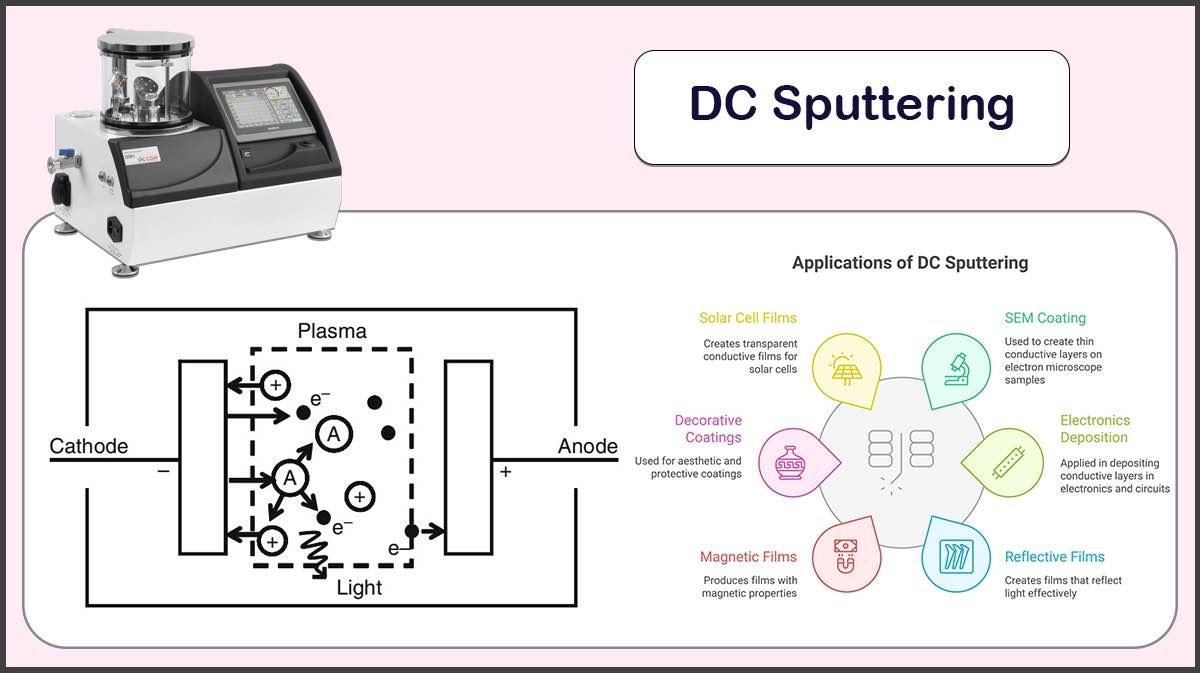
During the sputtering process, the surface of the sputtering target is bombarded by the positive ions generated in the plasma of the process gas.
The substrate ion bombardment can be controlled by adjusting the applied voltage, which can modify the direction and kinetic energy of the arriving particles to the substrate surface, thus controlling the penetration depth and achieving higher aspect ratio structures. Substrate bias also helps to increase the deposition rate.
Applying a negative bias voltage to the substrate (less negative than the target) causes positive ions to sputter the substrate surface, causing a more uniform angular distribution and density of the deposited thin film.
Introducing a positive bias voltage to the substrate is beneficial in the creation of an oxide bonding layer on the substrate, hence improving the subsequent layer adhesion to it.
RF Substrate Bias
RF substrate bias is appropriate if the substrate is non-conductive. Applying DC voltage to a non-conductive substrate causes the substrate to be charged due to the collision of the charged particles, that could disturb the deposited thin film.
Applications of Bias Sputtering
Applying a negative substrate bias voltage results in increased ion energy, enhancing some of the coating features, which should be optimised due to some drawbacks of this method, such as inducing high stress.
Substrate biasing also provides ionic cleaning of the substrate surface prior to the deposition process, called conditioning. Furthermore, UV photons generated in the plasma contribute to the photon biasing phenomenon, enhancing desorption of impurities from the substrate surface.
Substrate bias in sputtering deposition can improve the mechanical properties of the coating, improve adhesion to the substrate, higher mass density, better crystallinity, and higher surface roughness, as well as enhance electrical properties like lower electrical resistivity.
Also, substrate biasing is effective in various applications, including:
- Semiconductors
- Magnetic thin films
- Superconducting thin films
- Deposition of tantalum, niobium, tungsten, and aluminium thin films for microelectronics
Moreover, bias sputtering empowers redistribution of the sputtered atoms on the substrate surface, resulting in a levelled and smooth coating, even on 3D structures, which is beneficial in coating conducting thin films on electron microscope samples to achieve high-resolution images.
Bias Sputtering in Our Sputter Coaters
Bias sputtering, defined as applying voltage to the substrate during the sputtering process, is a technique to modify sputter-deposited thin film characteristics, featuring enhanced mechanical properties, electrical resistivity, and surface layer adhesion. Vac Coat sputter coaters can be supplied with the substrate bias option to improve the coating procedure and create thin films with desired structures. Vac Coat offers single and multiple cathode systems, such as DST1-300 and DST3, with the substrate bias option, which can be used in advanced research projects to produce novel thin film structures.
Some of Vac Coat's Products
References
- Seeman, James M. “Bias sputtering: its techniques and applications.” Vacuum 17.3 (1967): 129-137.
- Maissel, L. I., and P. M. Schaible. “Thin films deposited by bias sputtering.” Journal of Applied Physics 36.1 (1965): 237-242.
- Lee, Hwan-Chul, Jai-Young Lee, and Hyo-Jun Ahn. “Effect of the substrate bias voltage on the crystallographic orientation of reactively sputtered AlN thin films.” Thin Solid Films 251.2 (1994): 136-140.
- Ouis, Abousoufiane, and Michel Cailler. “Effects of substrate bias voltage on adhesion of DC magnetron-sputtered copper films on E24 carbon steel: investigations by Auger electron spectroscopy.” Journal of adhesion science and technology 27.21 (2013): 2367-2386.
- Vassallo, Espedito, et al. “Effect of Negative Substrate Bias Voltage and Pressure on the Structure and Properties of Tungsten Films Deposited by Magnetron Sputtering Technique.” Coatings 15.3 (2025): 319.
- Jang, Gil Su, Seon Mi Ahn, and Nong-Moon Hwang. “Effects of sputtering power, working pressure, and electric bias on the deposition behavior of Ag films during DC magnetron sputtering considering the generation of charged flux.” Electronic Materials Letters 18.1 (2022): 57-68.
- Brown, Hayley L., et al. “The impact of substrate bias on a remote plasma sputter coating process for conformal coverage of trenches and 3D structures.” Journal of Physics D: Applied Physics 48.33 (2015): 335303.

