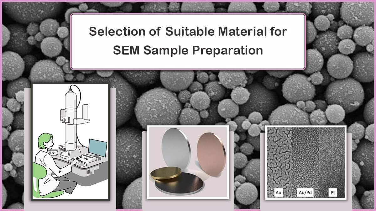
Selection of Suitable Material for Preparing an Electron Microscope Sample
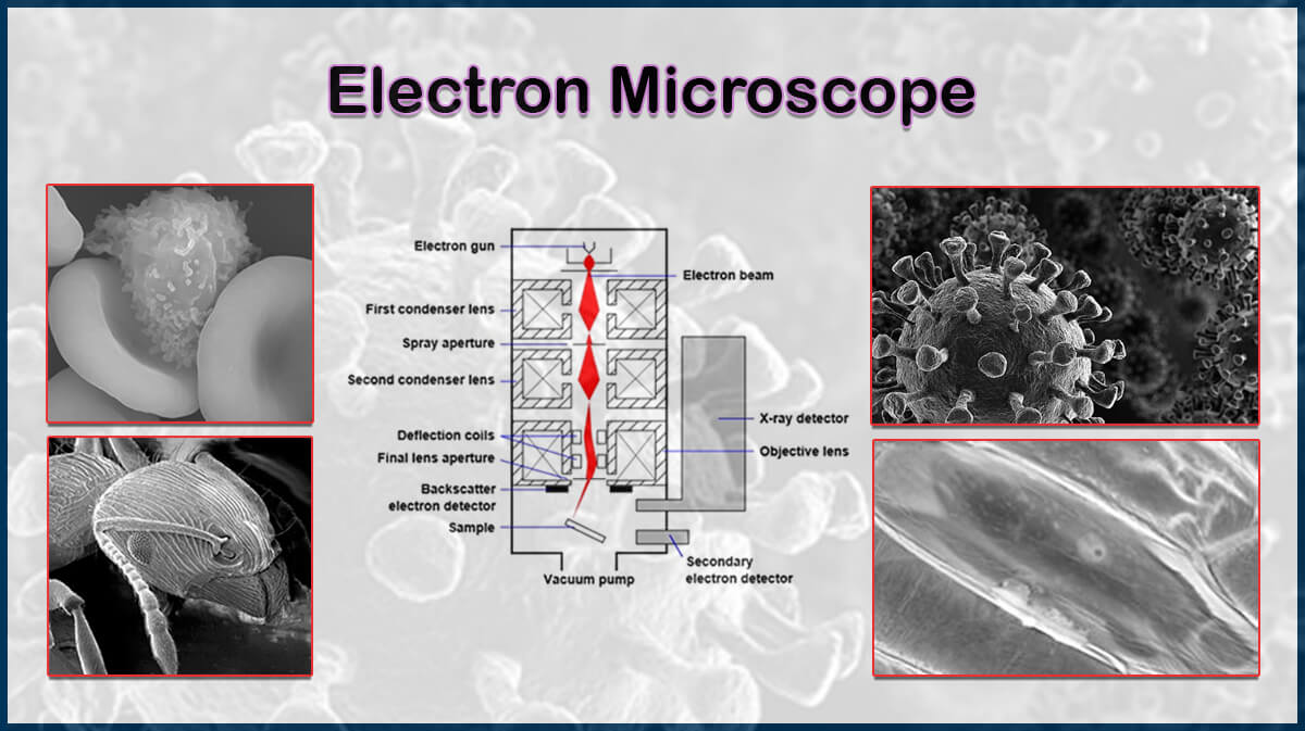
Electron microscopy (EM) is a comprehensive characterization tool to explore micro-nano structures. The samples under study should be prepared before imaging by any type of electron microscopy, namely SEM, FESEM, or TEM. Coating the sample surface with a thin film of proper material, selection material for SEM samples, is one of the well-known preparation steps to achieve high-resolution, clear images. Vac Coat offers various vacuum coaters for SEM sample preparation.
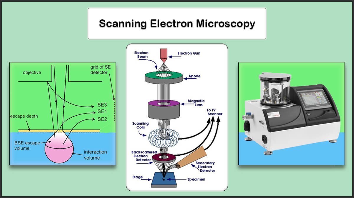
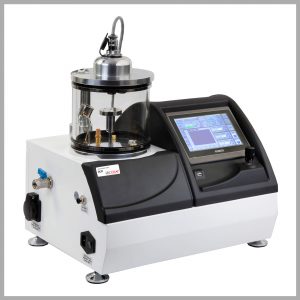
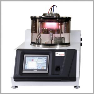
Vac Coat low vacuum sputter coater (DSR1), carbon coaters (DCR), and sputter and carbon coater (DSCR) are low-priced tabletop SEM sample coaters, used to create non-oxidizing coatings like gold, silver, and carbon.
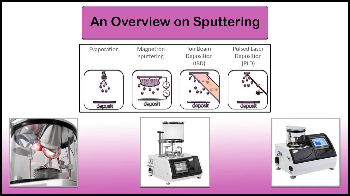
High vacuum SEM coaters equipped with a turbo molecular pump, such as DST1 sputter coater, DCT carbon coater, and DSCT sputter and carbon coater, enable coating the SEM samples with various materials, oxidizing or non-oxidizing. High vacuum coating also provides finer layer grain size, ideal for higher magnification imaging.
Which Samples Need Coating Before EM?
Sputter coating the sample for EM imaging is used in the case of:
- Beam-sensitive samples:
Beam-sensitive samples’ surfaces (like biological samples) may deteriorate when exposed to the high-energy electron beam, raising the need to cover the sample surface with a thin film of a protective layer.
- Non-conductive samples:
The incident electron beam on the non-conductive surface results in trapping the electrons and charging the surface, thus a thin, conductive coating helps to remove the excessive charge (Figure 1).

Coating Materials in Selection Material for SEM
Different materials have diverse coating properties and need deposition conditions. Materials with finer grain size and lower sputtering rates lead to enhanced image quality and resolution, suitable for high-resolution electron microscopic imaging. Also, oxidizing materials should be deposited under high vacuum conditions. Here is a brief description of the most common coating materials used for SEM/FESEM sample preparation.
Selection Material for SEM Samples
Gold (Au)
The most commonly used material to prepare samples for characterization by electron microscopy is gold. Gold provides high-quality microscopic images for above 30000X magnifications due to its high electrical conductivity and typically small grain size (Around 5 nm). Gold is a non-oxidizing material, so Vac Coat low vacuum sputter coating system DSR1 is a proper choice for SEM sample preparation.
Carbon (C)
For the EDX process, carbon is used instead of gold in selection material for SEM sample preparation process. Carbon has a small atomic number, and unlike gold, it does not add any peak to the X-ray spectrum of the specimens. Desktop carbon coating devices like DCR and DCT are favorable sample preparation systems for EDX analysis.
Platinum (Pt)
Platinum has a finer grain size compared to Au or Au/Pd coatings, with excellent SE (Secondary electron) yield, applicable for higher magnification imaging. Pt sputtering rate is nearly 60% lower than for Au, due to its higher work function. Pt coating drawbacks are higher fabrication costs, and its sensitivity to oxygen presence during coating, resulting in “stress cracking”.
Palladium (Pd)
Pd coating is suitable for low to medium-magnification imaging. It has a lower SE signal than Au. Pd is also an alternative to carbon coating when using EDX analysis. Palladium has the advantage of being able to dissolve and can be removed from the sample surface so that the sample can be returned to the pre-deposition condition.
Gold/Palladium (Au/Pd)
Au/Pd alloy with 60/40 or 80/20 ratios, has a lower sputtering rate in comparison with Au. Au/Pd is recommended to obtain a smaller grain size than a gold coating, especially when deposited under high vacuum conditions, achievable by DST1 sputter coaters. It is not recommended for EDX analysis due to the extra peaks for Pd.
Platinum/Palladium (Pt/Pd)
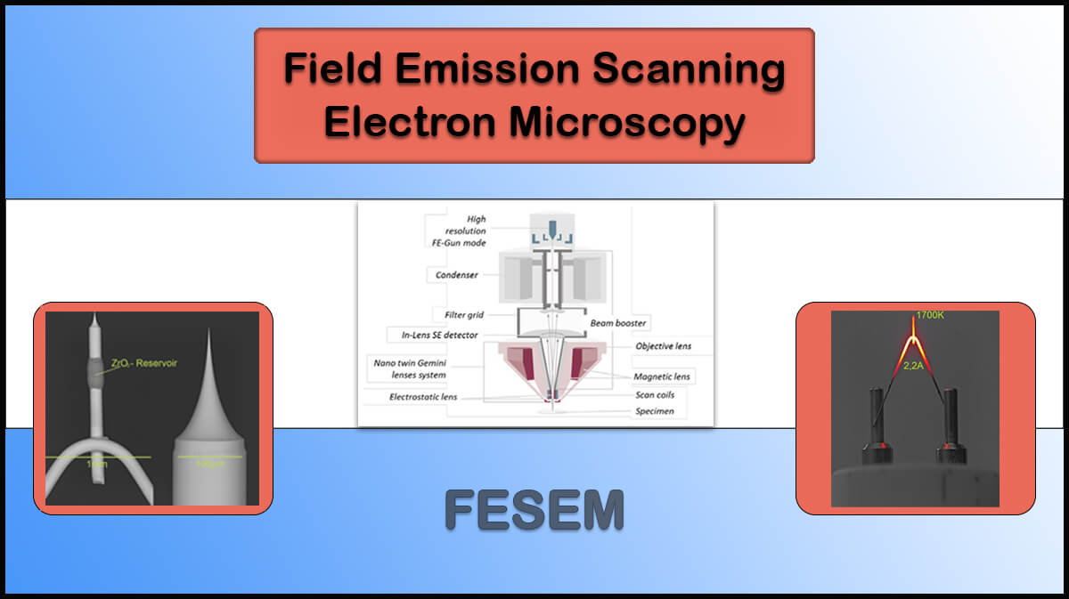
Pt/Pd alloy (80/20) resolves the platinum “stress cracking” problem, while its grain size and SE yield are the same as Pt. A high vacuum sputter-coated thin film of Pt/Pd is suitable for FESEM applications. DST1 turbo-pumped desktop sputter coater provides proper conditions for Pt/Pd deposition.
Chromium (Cr)
High vacuum sputter coated Cr on semiconductor materials is proved to have a very fine grain size, beneficial for FESEM applications. Also, Cr is a cost-effective material compared to other Au, Pd, or Pt. However, Cr is an oxidizing material, thus requiring a pre-sputtering process for target conditioning with a closed target shutter, and pure Argon flow into the chamber for oxygen removing and preventing oxidization of the sputtered Cr layer.
Also, it has a lower SE yield and sputtering rate than other materials which results in target heating. Cr is an excellent coating material for high-resolution backscattered electrons (BSE) imaging of materials with low atomic numbers (Z). DST1 turbo-pumped high vacuum sputter coater is able to perform programmable coating processes with pre-sputtering step and electronic target shutter control.
Also, they have many applications in industry and research including decorative coatings, biosensors, plasmonic devices, photovoltaic cells, batteries, and acoustic wave resonators.
Iridium (Ir)
Ir is a non-oxidizing, highly conductive material with a very fine grain size on almost all materials, excellent for high and ultra-high-resolution FESEM imaging. Ir has a high SE yield and low sputtering rate, needing a high-resolution sputter coater. Fabrication and coating costs are lower than for Pt or Pt/Pd. Ir as a rare material is an outstanding alternative coating material for sample analysis by EDX or WDX.
Tungsten (W)
W coating with very fine grain size, high SE yield, and a low sputtering rate is a proper, low-cost alternative for high-resolution coating. But it oxidizes rapidly, like Cr, so the samples must be kept under vacuum conditions and imaged immediately after coating.
Silver (Ag)
Ag is a more convenient, cost-effective alternative for Au, with nearly the same grain size and sputtering rate, and lower SE yield, suitable for low and medium magnifications imaging. Suitable for EDS analysis of P, Cl, and S-containing samples, Ag coating is also beneficial when the sample is required for further studies after imaging since it can be easily removed with Farmer’s reducer.

Limitation of Coating Electron Microscope Samples
Despite all the benefits of coating the EM samples as a preparation step with proper target material selection, it has its drawbacks.
- The coating process is technical, and achieving the right coating parameters may require an optimization procedure.
- The surface of the sample is covered with the coating, hence some information on the sample’s atomic number may be lost.
- Some features of the surface could be modified by the coating, and the sample’s pristine structure missed. So, control of sputter parameters is necessary to ensure that these problems are avoided.

Vac Coat Products
References
- Heu, Rod, et al. “Target material selection for sputter coating of SEM samples.” Microscopy Today 27.4 (2019): 32-36.
- J Goldstein, et. al., Scanning Electron Microscopy and X-ray Microanalysis, Kluwer Academic/Plenum Press, New York, 2003.
- https://www.microtonano.com/TIN-Target-material-selection-for-coating-SEM-samples-using-an-SEM-sputter-coater.php
- https://www.labtech-em.com/em/em-sputtering-metals-selection-guide
- https://ravescientific.com/education/37-proper-target-material-selection-when-coating-samples-using-an-sem-sputter-coater
- A comparative study of thin coatings of Au/Pd, Pt, and Cr produced by magnetron sputtering for FE‐SEM, https://doi.org/10.1046/j.1365-2818.1998.00282.x










What is the difference between Au/Pd 60/40 and 80/20 targets in sputtering deposition?
“1- The Au/Pd target has a lower cost as the Pd percentage increases in the target.
2- Since Pd has a higher work function compared to Au, increasing the Pd amount in the target results in a lower sputtering rate, hence finer grain size of the deposited layer. However, it is not suitable for heat sensitive samples.”