
Introduction
Ion beam sputtering (IBS) is a physical vapor deposition (PVD) method which provides the highest precision and control among all other thin film deposition methods like thermal evaporation, DC/RF magnetron sputtering and pulsed laser deposition (PLD). The high quality of IBS stems from low chamber pressure and high-energy ions striking the target(s). Offering various advantages from layer uniformity, stability, thickness control, and choice of material (metals, insulators, magnetic materials, refractory metals), ion beam sputtering is of interest to experts of optics, sensors (MEMS), thin film solar cells, and semiconductors.
Ion Beam Sputtering
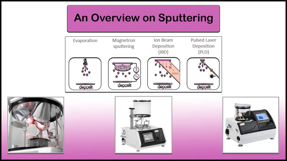
Ion beam sputtering (IBS), also known as ion beam deposition (IBD), is a thin film deposition technique to produce high-quality thin films of various materials ranging from metals to semiconductors and dielectrics. This deposition technique is widely used in the optics industry, where dense, uniform layers are essential. IBS offers the advantage of replicability, low impurity level of thin films along with strict control over the layer stoichiometry compared to thin films made by conventional magnetron sputtering (MS). In an IBS process, a broad beam of collimated ions strikes the target; as a result, target atoms (or molecules) are sputtered and then relax on the substrate.
Mechanism
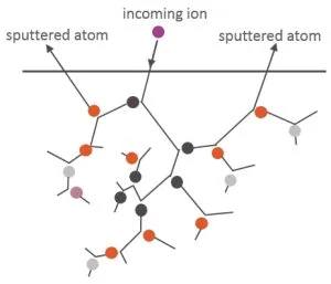
In a typical sputtering process, once the energetic inert gas (Argon or Xenon) ions hit the target, the atoms (or even molecules) of the target are knocked out. These ejected particles have high kinetic energy in the range of 1-10 eV and therefore form very compact, pinhole-free thin layer. A schematic of the sputtering process is displayed in Figure 1.
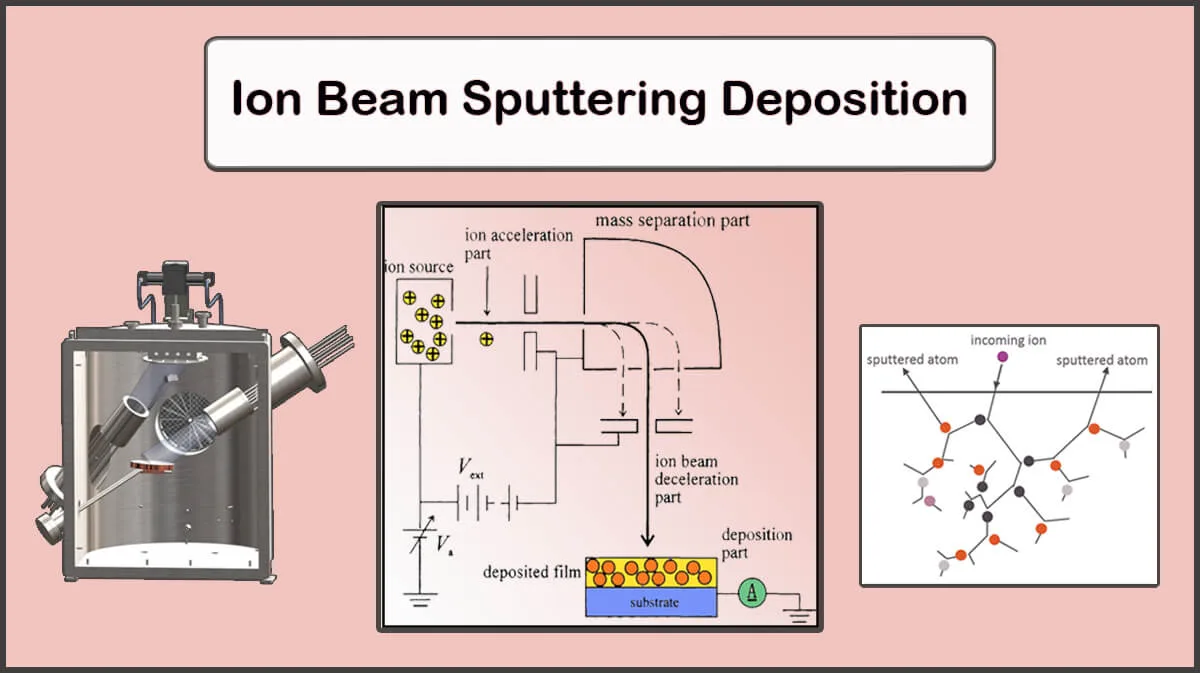
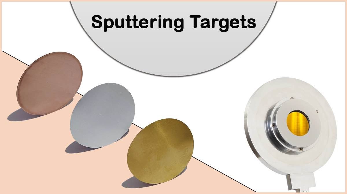
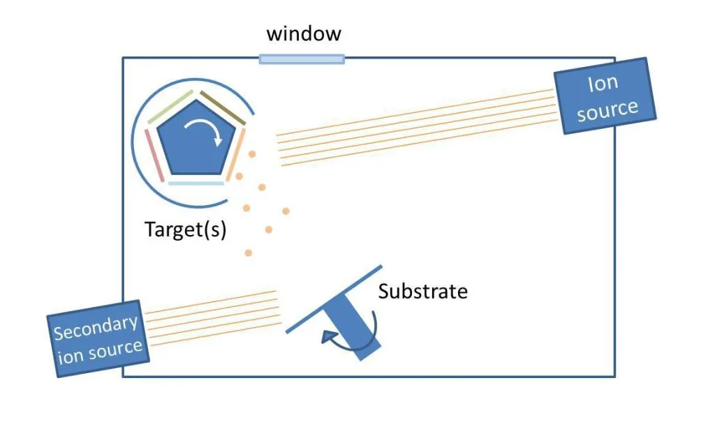
There are a number of key components inside an Ion Beam Sputtering Deposition chamber: 1. Ion source, 2. Target, and 3. Substrate holder as shown in Figure 2.
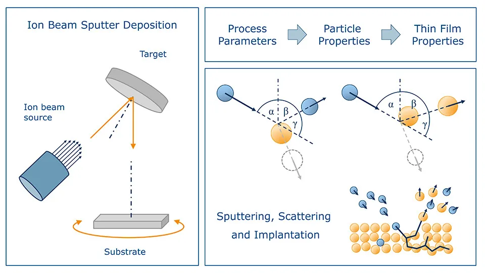
Ion Source in Ion Beam Sputtering Deposition
Inside the ion source, a high voltage of 2-10 kV is applied between the cathode and the anode with common central axis, which ionizes Argon (Ar) atoms. Positively charged Ar ions accelerate toward the grid or filament in the throat of ion source and leave it on their way towards the target. The ion source produces highly energetic beam and therefore, generates films with excellent adhesion and high packing density. Typical pressure during IBS process is about 10-4 Torr, which is lower than the nominal pressure of the conventional sputtering process. This is a result of delimiting Ar plasma inside the ion source, allowing lower pressures in the chamber, which is beneficial in lower impurity rate of the deposited film.
Kaufman Ion Source
A Kaufman ion source, also known as Kaufman-type gridded ion source, is a widely used source for ion beam sputtering deposition, which generates a highly collimated, mono-energetic ion beam of an inert gas, as Argon, toward the sputter target. Accordingly, Kaufman ion sources are ideal for optical coatings and precision research.
A Kaufman source involves several components:
- Discharge chamber, containing an inert gas (Typically Argon) for ionisation,
- Hot cathode or filament, from which the electrons are emitted to ionize a noble gas,
- Extraction grids, including two or three grid, the screen grid, accelerator grid, and optional decelerator grid, imposing an electrostatic potential difference to collimate and control the beam energy in the range of 100-1500 eV.
The ion energy and beam current are determined mainly by extraction voltage, discharge voltage, and grid spacing, following the Child-Langmuir Law for a given grid geometry:
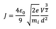
Where J is the current density, V is the acceleration voltage, d is the inter-grid spacing, and mi is the ion mass.
The energy of the extracted ions is given by the below equation (q= electric charge and Vacc= accelerating voltage), having a nearly monoenergetic distribution to achieve a uniform thin film.
Eion = q . Vacc
The generated positive ions in the hot cathode are confined by the magnetic field, forming a dense localized plasma, entering the grid system. The directed ion beam after passing through the grids collides the target to sputter its surface atoms.
Also, a neutralizer should be used to provide a matching electron current so as to prevent the target surface from charging effects.
However, gridded ion sources have limitations like grid erosion at high energies, limited filament lifetime, charge accumulations on the target, and higher cost and complexity compared to RF or end-Hall sources.
Ion Beam Sputtering Techniques
There are two other methods of utilizing ion beam sputtering for thin film deposition:
Ion Beam Assisted Deposition (IBAD)
In some cases, a secondary ion source is also utilized either to clean the substrate before the deposition or to perform ion beam assist deposition (IBAD). IBAD is of interest especially where metal oxide or nitride films are to be deposited since it improves the density, optical properties and moisture stability of the film. In IBAD the second ion source is referred to as Assist Ion Source.
Reactive Ion Beam Deposition (RIBD)
To perform reactive ion beam deposition (RIBD), a non-inert gas (i.e. O2 or N2) is introduced to the chamber, which reacts with the sputtered atoms to form oxide or nitride compound on the substrate.
The multi-target configuration enables the deposition of alloys or compounds from multiple targets in a single process. Rotating substrates during deposition enhances film uniformity. To improve the film quality further, rotary planetary substrate holders are favorable over single-rotation specimen stages.
Advantages of Ion Sputtering
Ion Sputtering is widely known to produce highest quality films in terms of performance and precision. This deposition method is used wherever film thickness, stoichiometry and uniformity are to be controlled strictly. Ion beam sputtering can produce smooth and dense thin films with thicknesses ranging from angstrom-scale to micrometers, excellent for precision optics. A major advantage of IBS over other sputtering methods is the control over several different parameters including ion energy, angle of incidence, and target sputtering rate almost independently. This enables enhanced process stability and stable deposition rates. Another important strength of IBSD is the possibility of coating different material classes from metals to insulators.
Drawbacks
Low deposition rate and high cost are considered as IBD disadvantages compared to other physical vapor deposition (PVD) methods.
Applications of IBD
Because of the numerous merits of IBD, including extremely uniform and very dense coatings, strong adhesion of thin film to the substrate, low-temperature and low-loss process, high damage threshold, and low-stress film forming, it is ideal for use in a wide range of applications, including:
- Optical coatings: such as optically smooth surfaces e.g. anti and high reflective filters, beam splitters, extreme UV (EUV) mirrors, laser facets
- Semiconductor production
- Deposition of high corrosion resistant films
- Flexible display industry
- Flat and smooth interfaces for multi-layer depositions as in metal oxides
- Transparent conductive oxides (TCO) depositions in the OLED
Ion Beam Sputtering Deposition (IBSD) is a highly precise thin-film deposition method that excels in uniformity, stability, and material control, making it ideal for optics, semiconductors, and nanostructure formation. Unlike conventional sputtering, IBS operates at lower chamber pressures, resulting in films with fewer impurities and better stoichiometry.



Vac Coat Sputter Coaters
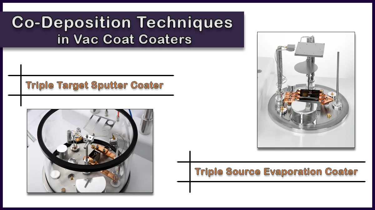
Vac Coat offers vacuum deposition systems using different coating methods, such as thermal evaporation, sputtering and pulsed laser deposition. Desktop low/high vacuum Vac Coat coating systems, can provide several deposition techniques in a single platform, including sputtering and carbon evaporation in DSCR/DSCT as well as metal evaporation in DSCT-T. These hybrid coating systems are ideal for electron microscopy sample preparation and contact layer coating, whereas more advanced triple target sputtering systems and thermal evaporation with angled/straight cathodes (DST3-TA/S) fulfill nearly all research demands.
Vac Coat Glovebox integrated sputtering system with thermal evaporation DST2-TG, has the full advantage of fast switching between the two deposition methods without breaking the vacuum.

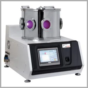
Some Of Vac Coat's Products


References
- https://polygonphysics.com/applications/ion-beam-sputter-deposition
- Bundesmann, Carsten, and Horst Neumann. “Tutorial: The systematics of ion beam sputtering for deposition of thin films with tailored properties.” Journal of Applied Physics 124.23 (2018): 231102.
- https://en.wikipedia.org/wiki/Ion_beam_deposition
- Ohashi, Kenya, Kiyoshi Miyake, and Tetsuroh Minemura. “Formation of high corrosion resistant iron films by ion beam deposition method.” Advanced Materials’ 93. Elsevier, 1994. 207-210.
- Miyake, K. (2002). Ion-Beam Deposition. In: Waseda, Y., Isshiki, M. (eds) Purification Process and Characterization of Ultra High Purity Metals. Springer Series in Materials Processing. Springer, Berlin, Heidelberg. https://doi.org/10.1007/978-3-642-56255-6_7
- H. R. Kaufman, “An ion source for broad-beam ion implantation,” Journal of Applied Physics, vol. 43, pp. 2080–2085, 1972.
- H. R. Kaufman and R. S. Robinson, “Ion sources for ion-assisted deposition,” Journal of Vacuum Science & Technology A, vol. 5, no. 4, 1987.
- H. Kaufman, “Technology and Applications of Broad-Beam Ion Sources,” AIP Conference Proceedings, 1989.
What physical phenomena occur when energetic particles impact a solid substrate to form thin films?
This thin film deposition technique is called Ion Beam Assisted Deposition (IBAD) and is discussed on our blog page https://vaccoat.com/blog/ion-beam-sputtering-ibsd/.