The Best Conductive Coating Thickness for Electron Microscopy and Microanalysis
Coating an insulating specimen with a thin conductive layer is one of the common sample preparation steps prior to the surface analysis techniques engaging electrons. A thin coating of a conductive material with proper grain size enhances charge dissipation on the sample surface that is bombarded by the electrons. Choosing the proper conductive coating thickness for electron microscopy and microanalysis, such as scanning electron microscopy (SEM), transmission electron microscopy (TEM), electron backscatter diffraction (EBSD), energy-dispersive X-ray spectroscopy (EDS/EDX), and wavelength-dispersive spectroscopy (WDS), helps to achieve a high-resolution imaging and precise examination of the sample’s surface.

How Thickness Of The Conductive Layer Affects The Imaging Result?
The coating layer quality, grain size, and homogeneity rely on various factors, including coating material, layer thickness, coating process conditions such as vacuum level, substrate temperature, process gas pressure and molecular weight, and accelerating voltage in case of sputter coating, as well as substrate composition and topography.
According to the proposed analysis technique and sample structure, different coatings with distinct thickness values can fit the application. The required thickness for the conductive layer covering the specimen surface strongly depends on several features like sample porosity, heat resistance, surface roughness, required analysis features, and other parameters that will be discussed in this article.
Effect of Conductive Coating Thickness on the Grain Size
Grain size of the conductive coating on an SEM sample is an important parameter in high-resolution imaging in scanning electron microscopy, where small grain size metals (Such as gold, iridium, molybdenum, tungsten) are preferred.
The grain size of the metallic thin film depends on several factors, including metal type, thin film thickness, and coating chamber pressure. Thin film grain size raises by an exponential power law in correlation with the film thickness, with the exponent depending on the perceived growth mechanism and zone. Thinner layer thicknesses result in smaller grains.
Effect of type of metal source and deposition chamber pressure on the grain size are studied in another blog articles.

Best Conductive Coating Thickness for SEM
Typical conductive coating thickness for SEM analysis is considered in the range of 2–20 nm. Utilizing the lower or upper limits as the proper thickness have advantages and challenges depending on the sample structure and analysis condition.
Coating a Thin Film on SEM Samples (Less than 5 nm)
Advantage: It can preserve the microscopic surface structure of the specimen through imaging. Furthermore, it allows less energetic electrons, such as backscattered electrons, to reach the detectors for further analysis. Additionally, EDS spectra the sample is less affected by the one from the conductive coating.
Challenge: A thin conductive film may not fully eliminate charge build up on the sample surface.
Coating a Thick Film on SEM Samples (More than 15 nm)
Advantage: It can fully cover up the insulating parts of the sample surface, especially in case of porous samples or extremely rough surfaces. Moreover, a highly conductive surface can protect beam-sensitive specimen from heating and deformation during imaging process. Also, the increased signals can yield a high-resolution image.
Challenge: It may obscure the microstructures of the specimen and hinder the low-energy electrons (as in case of secondary-electrons, SE, or backscattered electrons, BSE).
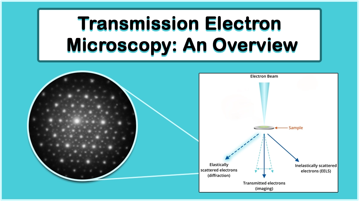
The Right Conductive Coating Thickness for TEM
Transmission Electron Microscopy (TEM) typically requires a thin conductive carbon coating on the TEM grid to support the sample during electron microscopy imaging process, as well as a thin conductive layer on the non-conductive samples to prevent charging effect. Usually an ultrathin <3 nm support film is needed for high-resolution imaging and around 5nm thin carbon film for sample preparation.
Proper Conductive Coating Thickness for Microstructure Analysis
Nowadays, most research samples and industrial products in various fields require microanalysis of the sample structure to reach the best performance, most of which contain electron beam emission onto the sample surface. Therefore, coating the specimen with a thin conductive film seems vital to achieve an accurate result, but the proper thickness of the coating depends on the type of electron analysis and the sample structure. In the following, the proper coating thickness for the conductive layer to achieve high-quality electron microanalysis and spectroscopy is reviewed.
EBSD (Electron Backscattering Diffraction)
For EBSD analysis, a too thin conductive coating won’t be sufficient to dissipate the charge, while a thick one decreases the signal to noise ratio significantly and result in very poor result. Typically, a 2-5 nm coating works for charge dissipation and maintaining high signal-to-noise ratio EBSD signal. The best conductive coating thickness for EBSD is beneficial to preserve the elemental difference when generating elemental contrast by the backscatter detector. The coating could be sputtered or evaporated carbon, or other materials such as gold or tungsten. A 5-10 nm carbon layer coating on non-conducting samples is required for optimized SEM condition for EBSD analysis.


EDS or EDAX (Electron Diffraction X-Ray Spectroscopy)
The thinner conductive coating minimizes impact on EDS spectra. A carbon coating of about 2–5 nm is preferred to prevent charging and minimize peak overlap in EDS analysis, while metal coatings, like Au and Pt, increase X-ray peak overlaps and absorption.
WDS (Wavelength Diffraction Spectroscopy)
Similar to the previous methods for sample preparation for the electron microanalysis, electrically insulating samples can be carbon-coated, mostly by carbon evaporation, to ensure conduction of the specimen surface while the conductive ones need not be coated. Since carbon layer can absorb low-energy X-rays significantly, affecting light element analysis, Al coating has also been suggested.
The Key Role of Coating Thickness in Electron Microscopy
In this article, the importance of the proper conductive coating thickness for electron microscopy is discussed. The optimized conductive layer thickness improves image quality and sensitivity in electron microscopy and microanalysis.
The uniformity and thickness control of the conductive coating are proven to be critical for reproducibility and analytical accuracy in SEM, TEM, EDS, EBSD, and WDS analysis.
Gold and gold/palladium coatings were consistently reported to provide high-quality imaging and analytical stability, especially for biological tissues and high-precision applications, while for TEM and EDS analysis, carbon coating is more common.
Typical thicknesses of the coatings are in the range of 2-50 nm, where the best conductive coating thickness for EM is determined by the sample structure and the target analysis.
Vac Coat SEM and Carbon Coaters
Vac Coat offers various SEM coaters featuring QCM thickness sensors, rotational and planetary rotating sample stages, automatic deposition processes, and real-time process monitoring, that can provide reproducible conductive thin films with nanometre thickness. DSR1 and DST1 are ideal for metal coatings on electron microscope samples, whereas DCR and DCT are perfect carbon coaters for TEM grid coating and EDS analysis. Hybrid coating systems, such as DSCR and DSCT, enable both sputter coating and carbon evaporation to supply a versatile coating experience for researchers.

Some of Vac Coat's Products


References
- Höche, J. Gerlach, and T. Petsch. “Static-Charging Mitigation and Contamination Avoidance by Selective Carbon Coating of TEM Samples.” Ultramicroscopy, 2006.
- Yun Xu, Fan Zhang, and Fairy Chen. “Study of Coating Effect on TEM Sample Damage and Elemental Analysis.” China Semiconductor Technology International Conference, 2024.
- https://www.jeol.com/applications/pdf/sm/sem_atoz_all.pdf
- https://warwick.ac.uk/research/rtp/em/info/specimenpreparation.pdf
- https://www.ebsd.com/hints-and-tips/ebsd-sample-preparation/preventing-charging-coating
- https://www.struers.com/-/media/Library/Brochures/English/Application-Note-EBSD.pdf
- Walkiewicz. “Ultrathin Metal Coatings as a Solution for Successful SEM Imaging of Nano-Electrospinning Fibers.” Proceedings of the Microscience Microscopy Congress 2023 Incorporating EMAG 2023, 2023.
- https://kindle-tech.com/faqs/how-thick-is-sputter-coating-sem?srsltid=AfmBOorKalDKtlQu0EcYSvEyidlHDmHnVDNn6C1Vm83tBtluVVfv0XLg
- https://kindle-tech.com/faqs/how-thick-is-carbon-coating-for-sem?srsltid=AfmBOooNckCCxKpBkE8n-ST6EsFCWJhZ0r-AdKQ0vgN9ergrnjpQ4_4Y
- https://www.leica-microsystems.com/science-lab/life-science/brief-introduction-to-coating-technology-for-electron-microscopy/
- https://www.nanoscience.com/blogs/how-does-coating-thickness-affect-sem-imaging/
- https://www.jeolusa.com/RESOURCES/Sample-Preparation/Documents-Downloads/sample-coating-for-sem#:~:text=Traditional%20methods%20of%20dealing%20with,buildup%20and%20minimize%20beam%20damage.
- https://jeolusa.s3.amazonaws.com/resources_sp/Sample%20Coating%20for%20SEM.pdf?AWSAccessKeyId=AKIAQJOI4KIAZPDULHNL&Expires=2145934800&Signature=DJGMwbZkPGvz%2B4vkGsHMDV0nbXc%3D
- https://www.gu.se/en/core-facilities/sem-sample-preparation-techniques#:~:text=To%20prevent%20charge%20buildup%20on,to%20obscure%20specimen%20surface%20details.
- https://www.azom.com/article.aspx?ArticleID=22267
- https://www.ebsd.com/hints-and-tips/optimization-sem-condition
- https://www.ebsd.com/hints-and-tips/ebsd-sample-preparation/preventing-charging-coating
- https://www.tedpella.com/Support_Films_html/Support_Films_and_Substrates_Overview.aspx
- https://dspace.mit.edu/bitstream/handle/1721.1/82646/12-141-january-iap-2010/contents/lecture-notes/MIT12_141IAP10_coursenotes.pdf
- Chatterjee, Nilanjan, and Timothy L. Grove. “12.141 Electron Microprobe Analysis by Wavelength Dispersive X-ray Spectrometry, January (IAP) 2006.” (2006).
- Stokroos, Kalicharan, Van Der Want, and Jongebloed. “A Comparative Study of Thin Coatings of Au/Pd, Pt and Cr Produced by Magnetron Sputtering for FE‐SEM.” Journal of Microscopy, 1998.
- Dulmaa, Altangerel, et al. “On the grain size-thickness correlation for thin films.” Acta Materialia 212 (2021): 116896. Kondo, Toshiyuki, et al. “Thickness dependence of grain boundary strengthening effect on plasticity of submicrometer-to nanometer-thick freestanding copper thin films.” Materials Science and Engineering: A 931 (2025): 148193.
- https://www.emsdiasum.com/7a-holey-carbon-film-2?srsltid=AfmBOoqale78M_4Gj7RQ4yGeP6_HmM8hPZqJkraeLA34Qo8mQdNc9zI3
- Sikora, M., and D. Wojcieszak. “Impact of carbon and platinum protective layers on EDS accuracy in FIB cross-sectional analysis of W/Hf/W thin-film multilayers.” Micron 186 (2024): 103689.