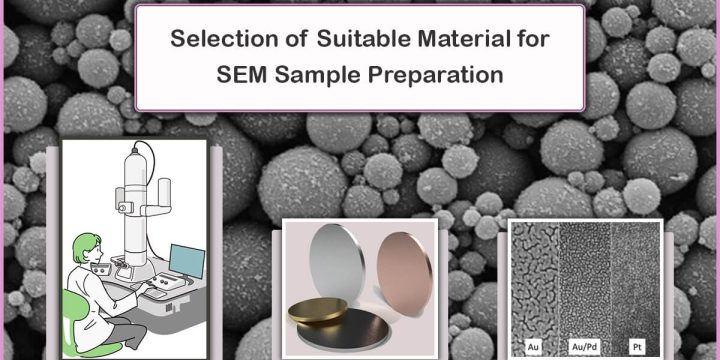
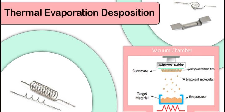
Unseen Universe by James Webb Space Telescope

Unseen Universe by James Webb Space Telescope

Report
[vc_row][vc_column width="3/4"][vc_row_inner][vc_column_inner][vc_column_text] James Webb Space Telescope First Infrared Images of the Unseen Universe The NASA’s James Webb Space Telescope has revealed first full-color images and spectroscopic data of distant galaxies, looking back to the beginning of the cosmic time. [/vc_column_text][/vc_column_inner][/vc_row_inner][vc_row_inner][vc_column_inner][vc_video link="https://youtu.be/JzDWpvtDJ9g" el_width="70" align="center"][/vc_column_inner][/vc_row_inner][vc_column_text css=".vc_custom_1715534184563{margin-top: -40px !important;}"] Thousands of Never Seen Before Galaxies! The Latest James Webb Space Telescope Image Explained in 4K [/vc_column_text][vc_row_inner css=".vc_custom_1715534207680{background-color: #d9d9d9 !important;}"][vc_column_inner width="2/3"][vc_column_text] How James Webb Telescope Works? James Webb Space Telescope detects young galaxies by observing distant ones, which are over 13 billion light years away from earth. To see such far-off and indistinct objects, a large mirror is needed. In other words, how much detail a telescope can see is related to the size of the mirror area collecting light from the observed object.…
Read More
Field Emission Scanning Electron Microscopy (FE-SEM)

Field Emission Scanning Electron Microscopy (FE-SEM)

Report
[vc_row][vc_column width="3/4"][vc_row_inner][vc_column_inner][vc_column_text css=""] What is Field Emission Scanning Electron Microscope (FE-SEM)? With the advancement of technology used in Scanning Electron Microscopy (SEM), a type of electron microscope, higher resolution images became available with the advent of Field Emission Microscopy in 1936 by Erwin Muller, resulting in the emergence of a new technique named as Field Emission Scanning Electron Microscopy (FE-SEM). [/vc_column_text][/vc_column_inner][/vc_row_inner][vc_row_inner css=".vc_custom_1715097622318{background-color: #d9d9d9 !important;}"][vc_column_inner width="1/2"][vc_video link="https://youtu.be/VWxYsZPtTsI" align="center"][vc_column_text css=".vc_custom_1715097734212{margin-top: -20px !important;}"] How a Scanning Electron Microscope Works? [/vc_column_text][/vc_column_inner][vc_column_inner width="1/2"][vc_cta h2="" txt_align="center" style="3d" color="mulled-wine" add_button="bottom" btn_title="What is SEM?" btn_style="3d" btn_color="juicy-pink" btn_align="center" btn_link="url:https%3A%2F%2Fvaccoat.com%2Fblog%2Fscanning-electron-microscope-sem%2F|title:Scanning%20Electron%20Microscope%20(SEM)"][/vc_cta][/vc_column_inner][/vc_row_inner][vc_row_inner][vc_column_inner width="1/2"][vc_column_text] FESEM Working Principles The method of operation of these microscopes is similar to that of conventional scanning electron microscopes (SEM). An electron beam focused by electromagnetic lenses scans the surface of specimen, where the reflected/interacted electrons create an image…
Read More
Scanning Electron Microscope (SEM)

Scanning Electron Microscope (SEM)

Report
[vc_row][vc_column width="3/4"][vc_row_inner][vc_column_inner][vc_column_text] What is Scanning Electron Microscopy? Scanning electron microscopy is an efficient and non-destructive technique that provides detailed information on the morphology, composition, and structure of the studied materials. The first one of this electron microscope was invented in 1942. It was shown at that time that Secondary Electrons (SE) produced topographic contrast using the collector positive bias rather than the sample. After that, many changes were made until the first commercial sample of scanning electron microscope was introduced in 1965. [/vc_column_text][/vc_column_inner][/vc_row_inner][vc_row_inner css=".vc_custom_1706461362914{background-color: #d9d9d9 !important;}"][vc_column_inner width="1/2" css=".vc_custom_1706463891655{margin-top: 20px !important;}"][vc_video link="https://youtu.be/Vs360UarP1U" align="center"][vc_column_text css=".vc_custom_1715592510407{margin-top: -30px !important;}"] Scanning Electron Microscope [/vc_column_text][/vc_column_inner][vc_column_inner width="1/2"][vc_cta h2="" txt_align="center" style="3d" color="mulled-wine" el_width="xl" add_button="bottom" btn_title="What is Electron Microscope?" btn_style="3d" btn_color="juicy-pink" btn_align="center" btn_link="url:https%3A%2F%2Fvaccoat.com%2Fblog%2Felectron-microscope%2F|title:What%20is%20an%20Electron%20Microscope%3F"][/vc_cta][/vc_column_inner][/vc_row_inner][vc_row_inner][vc_column_inner][vc_column_text] An Overview of Scanning Electron Microscopy In this microscopy, two classes of electrons are detected: secondary…
Read More
What is Pulsed Laser Deposition (PLD)?

What is Pulsed Laser Deposition (PLD)?

Report, Pulsed Laser deposition
[vc_row][vc_column width="3/4"][vc_row_inner][vc_column_inner][vc_column_text] An Overview of Pulsed Laser Deposition Pulsed laser deposition is a physical vapor deposition technique in which a high-energy laser is focused on a target material in a vacuum chamber and converted to a plasma plume, which is deposited on a substrate (Figure 1). The deposition can be assisted by a flow of oxygen or other background gases, or occur under ultra-high vacuum conditions. [/vc_column_text][/vc_column_inner][/vc_row_inner][vc_row_inner css=".vc_custom_1715269871382{background-color: #d9d9d9 !important;}"][vc_column_inner width="1/2"][vc_video link="https://youtu.be/JL8qvTW-WCg" align="center"][vc_column_text css=".vc_custom_1715271079446{margin-top: -20px !important;}"] Pulsed Laser Deposition PLD Explained with Animations [/vc_column_text][/vc_column_inner][vc_column_inner width="1/2"][vc_cta h2="" txt_align="center" style="3d" color="mulled-wine" el_width="xl" add_button="bottom" btn_title="What Is PVD?" btn_style="3d" btn_color="juicy-pink" btn_align="center" btn_link="url:https%3A%2F%2Fvaccoat.com%2Fblog%2Fphysical-vapor-deposition-pvd%2F|title:Physical%20Vapor%20Deposition%20(PVD)|target:_blank"][/vc_cta][/vc_column_inner][/vc_row_inner][vc_row_inner][vc_column_inner width="1/2"][vc_column_text] While the equipment needed to perform the deposition in this manner is roughly similar to other deposition methods (such as sputtering), the physical interaction between the laser beam and the target…
Read More
What is Plasma?

What is Plasma?

Report
[vc_row][vc_column width="3/4"][vc_row_inner][vc_column_inner][vc_column_text css=""] Plasma Physics Plasma is the fourth state of matter that can be reached in high energies. Normally, when atoms in a solid gain enough energy it goes to liquid phase, and then the phase transition is continued to the gas phase at higher energy levels, and then plasma is formed at extremely high temperatures. In a typical plasma, some or all of the electrons in an atom gain enough energy to overcome nucleus potential barrier and an ionized gas is formed. So, plasma contains free electron-ions and is able to conduct electricity. Since atoms are normally neutral, the plasma is electrically neutral. Plasma may contain magnetic fields as moving electric charges create them. [/vc_column_text][/vc_column_inner][/vc_row_inner][vc_row_inner css=".vc_custom_1713565210840{background-color: #d9d9d9 !important;}"][vc_column_inner width="1/2"][vc_video link="https://youtu.be/94tReSbyPYc"][vc_column_text css=".vc_custom_1713565196254{margin-top: -20px !important;}"] What is Plasma? [/vc_column_text][/vc_column_inner][vc_column_inner width="1/2"][vc_cta…
Read More
Electron Microscope Invention: A Historical Overview

Electron Microscope Invention: A Historical Overview

Report
[vc_row][vc_column width="3/4"][vc_row_inner][vc_column_inner][vc_column_text] History of Electron Microscope (1930-1980) Nowadays, the electron microscope is an essential instrument to characterize new structures and materials and electron microscope invention has become a popular topic for scientific research. In a typical electron microscope a beam of electrons is focused upon a target specimen. Information is often gathered from electrons transmitted through or scattered from the specimen by Bragg diffraction, alongside data gathered from Auger electrons, characteristic x-rays, and the charge absorbed by the specimen. On the basis of particle-wave duality theory of de Broglie, electrons can replace photons in a microscope to improve the image resolution more than 5000 times. [/vc_column_text][/vc_column_inner][/vc_row_inner][vc_row_inner css=".vc_custom_1715593366791{background-color: #d9d9d9 !important;}"][vc_column_inner width="1/2"][vc_video link="https://youtu.be/ljTEG-B-kGc" align="center"][vc_column_text css=".vc_custom_1715593799395{margin-top: -20px !important;}"] The Principle of the Electron Microscope [/vc_column_text][/vc_column_inner][vc_column_inner width="1/2"][vc_cta h2="" txt_align="center" style="3d" color="mulled-wine" add_button="bottom" btn_title="More About"…
Read More
Tin Dioxide Thin Film by Unbalanced Magnetron Sputtering

Tin Dioxide Thin Film by Unbalanced Magnetron Sputtering

Report, Sputtering
[vc_row][vc_column width="3/4"][vc_row_inner][vc_column_inner][vc_column_text] Case Study: The Role of Unbalanced Magnetron Sputtering on the Characteristics of Tin Dioxide Thin Film Indian researchers have succeeded in improving the optical, electrical, and structural properties of tin dioxide thin film by investigation the effect of using unbalanced magnetron sputtering on the properties of tin dioxide thin film. [/vc_column_text][/vc_column_inner][/vc_row_inner][vc_row_inner css=".vc_custom_1715594950177{background-color: #d9d9d9 !important;}"][vc_column_inner width="1/2"][vc_video link="https://www.youtube.com/watch?v=xjEOoKi6qUo" align="center" css=".vc_custom_1715595330762{border-radius: 2px !important;}"][vc_column_text css=".vc_custom_1715594925919{margin-top: -20px !important;}"] How Triple Target Sputter Coater DST3-A Works? [/vc_column_text][/vc_column_inner][vc_column_inner width="1/2"][vc_cta h2="" txt_align="center" style="3d" color="mulled-wine" add_button="bottom" btn_title="Thin Films Types" btn_style="3d" btn_color="juicy-pink" btn_align="center" btn_link="url:https%3A%2F%2Fvaccoat.com%2Fblog%2Fthin-film-and-thin-films-types%2F|target:_blank"] [/vc_cta][/vc_column_inner][/vc_row_inner][vc_row_inner][vc_column_inner][vc_column_text] Tin dioxide (SnO2), has received significant attention due to its potential applications in various fields such as coatings, energy harvesting, sensors, and electronic devices. Since the characteristics of the thin films depend on the conditions of the deposition and deposition methods, a lot of studies have been…
Read More
What is RF Sputtering? | DC vs RF Sputtering

What is RF Sputtering? | DC vs RF Sputtering

Report, Sputter Coater, Sputtering
[vc_row][vc_column width="3/4"][vc_row_inner][vc_column_inner width="1/2"][vc_column_text css=""] Why RF Magnetron Sputtering? Direct current (DC) sputtering is a cost-effective method for thin layer deposition of electrically conductive metallic targets. But this method is not applicable for non-conductive dielectric target materials, since bombarding such targets with positive ions causes charging the surface of the target, which repels further positive ion bombarding the surface, resulting in the cessation of sputtering process and arcing into the plasma. In order to overcome DC sputtering shortcomings, RF sputtering is widely used for electrically non-conductive target materials deposition. [/vc_column_text][/vc_column_inner][vc_column_inner width="1/2"][vc_column_text css=""] [lwptoc backgroundColor="#d6d6d6" borderColor="#5b5b5b" skipHeadingText="References|Recent Posts|RF Sputtering Systems|The Other Sputter Coaters|What is SEM?|FESEM vs SEM"] [/vc_column_text][/vc_column_inner][/vc_row_inner][vc_row_inner css=".vc_custom_1715789177436{background-color: #d9d9d9 !important;}"][vc_column_inner width="1/2"][vc_video link="https://youtu.be/sz5P0D8JZi4?si=i1uuV41yoflsilpK" align="center" css=".vc_custom_1741299405278{border-radius: 2px !important;}"][vc_column_text css=".vc_custom_1741299430011{margin-top: -20px !important;}"] Vac Coat Sputter Coaters [/vc_column_text][/vc_column_inner][vc_column_inner width="1/2"][vc_cta h2="" txt_align="center" style="3d" color="mulled-wine" add_button="bottom" btn_title="What…
Read More
Effect of Chamber Ultimate Pressure on Carbon Coating

Effect of Chamber Ultimate Pressure on Carbon Coating

Carbon Coater, Report
[vc_row][vc_column width="3/4"][vc_row_inner][vc_column_inner][vc_column_text] Effect of Chamber Ultimate Pressure on Carbon Coating Electron microscopy is a method to image samples, which provides much higher resolution and further details compared to traditional optical microscopes. Samples should be conductive for this analysis, so a conductive layer is normally deposited on the sample surface to image nonconductive surfaces. Carbon is one of the common materials used for sample preparation for electron microscopy, but carbon coating needs a vacuum chamber to reach required conductivity [1]. [/vc_column_text][/vc_column_inner][/vc_row_inner][vc_row_inner][vc_column_inner width="1/2"][vc_video link="https://youtu.be/j91sE_ZwJWM" align="center" css=".vc_custom_1716721853667{border-radius: 2px !important;}"][vc_column_text css=".vc_custom_1716721761116{margin-top: -20px !important;}"] How Does A Carbon Coater Work? [/vc_column_text][/vc_column_inner][vc_column_inner width="1/2"][vc_cta h2="" txt_align="center" style="3d" color="mulled-wine" add_button="bottom" btn_title="Carbon Coating" btn_style="3d" btn_color="juicy-pink" btn_align="center" btn_link="url:https%3A%2F%2Fvaccoat.com%2Fblog%2Fcarbon-coating-for-em-edx-sample-preparation%2F|title:Carbon%20Coating%20for%20EM%20and%20EDX%20Sample%20Preparation|target:_blank"] [/vc_cta][/vc_column_inner][/vc_row_inner][vc_separator][vc_row_inner][vc_column_inner][vc_column_text] Carbon can be coated in a low-vacuum or high vacuum system, choosing each results in different coating structure. In a typical…
Read More
Balanced and Unbalanced Magnetron Sputtering

Balanced and Unbalanced Magnetron Sputtering

Report, Sputter Coater, Sputtering
[vc_row][vc_column width="3/4"][vc_row_inner][vc_column_inner][vc_column_text css=""] Balanced and Unbalanced Magnetron Sputtering Sputtering was first introduced in 1852 and was used by a person named Groe. He could using an electrical discharge deposited the metal film on a cold cathode. At first, sputtering was used for deposition of the refractory metals film, whose deposition was not possible by thermal evaporation, but gradually, using radio frequency waves (RF Sputtering), the possibility of dielectric films was also provided by the sputtering deposition method. [/vc_column_text][/vc_column_inner][/vc_row_inner][vc_row_inner css=".vc_custom_1743259804428{background-color: #D9D9D9 !important;}"][vc_column_inner width="1/2"][vc_video link="https://www.youtube.com/watch?v=R-oNxgmgbJg" align="center" css=".vc_custom_1743259788547{border-radius: 2px !important;}"][vc_column_text css=".vc_custom_1655790224831{margin-top: -20px !important;}"] Gencoa Circular FFE Magnetron [/vc_column_text][/vc_column_inner][vc_column_inner width="1/2"][vc_cta h2="" txt_align="center" style="3d" color="mulled-wine" add_button="bottom" btn_title="Thermal Evaporation" btn_style="3d" btn_color="juicy-pink" btn_align="center" css="" btn_link="url:https%3A%2F%2Fvaccoat.com%2Fblog%2Fthermal-evaporation-method%2F|title:Thin%20Film%20Deposition%20By%20Thermal%20Evaporation%20Method|target:_blank"] [/vc_cta][/vc_column_inner][/vc_row_inner][vc_row_inner][vc_column_inner][vc_column_text css=""] Sputtering is in fact the process of transferring the momentum of the particles (usually the ions of neutral gases) to the surface of the target. Parameters such as…
Read More