Chalcogenide Thin Films Deposition
Chalcogenides are materials that contain at least one of the chalcogens, elements of group 16 of the periodic table (Sulfur, selenium, tellurium, etc.). Chalcogenide binary, ternary, and quaternary derivatives are widely employed in photovoltaic, photocatalyst, sensor, fuel cell, and battery fabrication.
Chalcogenides’ Properties
Chalcogenide compounds, such as transition metal chalcogenides, contain chalcogen anions like S2−, Se2−, or Te2−, and at least an electropositive element. Chalcogenides have a narrow band-gap energy which results in special optical properties of chalcogenide glasses, such as high refractive index, infrared (IR) transparency, nonlinear optical properties, and reversible phase change from amorphous to crystalline. Chalcogenide glasses can be polished or machined into planar, spherical or other shapes for various applications.
Chalcogenides’ Thin Films Applications
Chalcogenide thin films are used in a variety of applications for their narrow band-gap energy, non-toxicity, bio-compatibility, economical and facile synthesis. Chalcogenide thin films can be used in producing:
- Photovoltaic cells
- Solar Cells
- Fuel Cells
- Batteries
- Gas Sensors
- Supercapacitors
- Optical imaging
- Hologram recording
- Optical mass memories
- IR fiber optics

Chalcogenide Thin Film Deposition Methods
Optical properties and other characteristics of thin films (Thermal, mechanical, resistance, chemical, photo-sensitivity, etc.) are highly dependent on the deposition methods. Depending on how the thin film is deposited, the stoichiometry, structure, defect states, and many other features can be controlled. Chalcogenide thin films can be deposited by chemical or physical routs like physical vapor deposition (PVD) techniques.

Chemical Deposition of Chalcogenide Thin Films
The chalcogenides can be deposited in the chemical processes from the gas phase, called Chemical Vapor Deposition (CVD). In this method, the gaseous precursors react in the gas phase or at the substrate–gas interface to produce a thin film on the substrate, so the composition of the thin film is different from the gases. CVD technique has the advantages of creating a film with a uniform thickness (and composition), using high-purity precursors, and high deposition rates (approx. 1 μm/min). However, this deposition technique has its drawbacks, such as being a high-temperature process and limited range of materials that can be coated through this method.
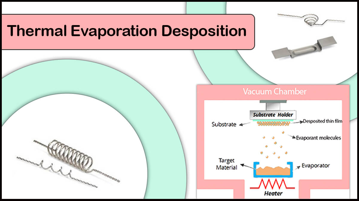
Thermal Evaporation
Thermal evaporation method is used for the deposition of the binary Chalcogenide materials such as As-S (Se) and Ge-S (Se). This method is also used for the deposition of Amorphous Selenium for use in X-ray sensitive flat panels. Thermal evaporation is very popular among thin film deposition methods due to its simplicity and low-cost, reproducibility, excellent process control, and the ability to coat elemental, alloy and compound coatings on substrates with a large area.
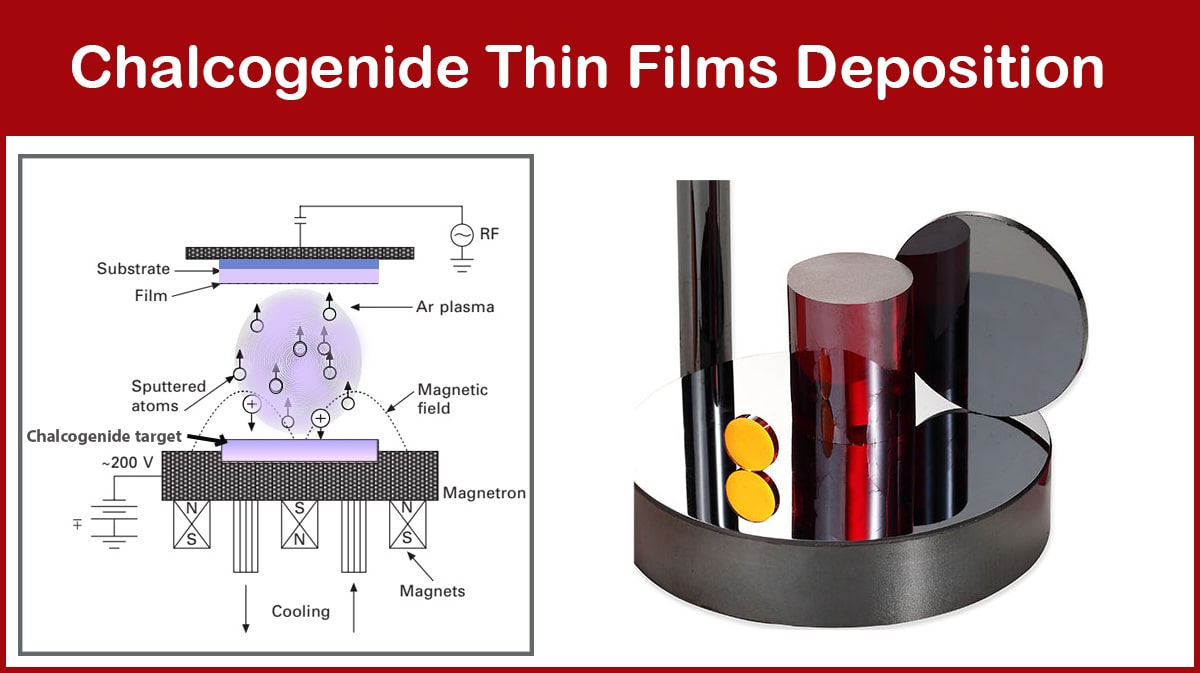
Sputtering in Chalcogenide Thin Films Deposition
Sputtering is one of the most appropriate methods for a wide range of Chalcogenide thin films applications. It can be used for deposition of binary (e.g. a-Ge-Te), ternary (e.g. a-Ge-Ga-S), or multi-component (e.g. a-Ag-In-Sb-Te) glasses. Sputtering is the principal industrial technique that is used for deposition of chalcogenide films for optical and electrical data-storage applications.
Thickness uniformity control is best achieved in all substrate areas using the sputtering method, but the deposition rate of Chalcogenide materials is low with this method and is less than 1 nm per second. Because most Chalcogenide materials have low electrical conductivity, the use of RF sputtering and back-plated targets are recommended for these materials.
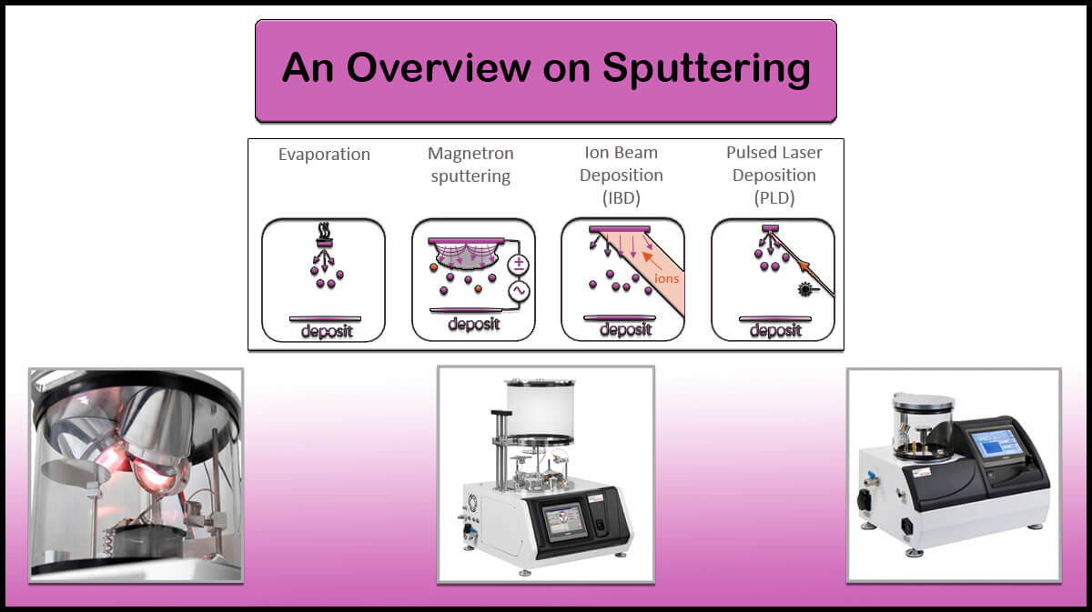

Pulsed Laser in Chalcogenide Thin Films Deposition
The Pulsed Laser Deposition (PLD) method has also been used to deposit thin films of Chalcogenides. One of the advantages of using this method is the deposition of thin films with completely the same stoichiometry as the target material, although, this feature depends on the pulse power density. Different deposition conditions also affect the structure of PLD films. The high energy of the ablated species results in high density and good adhesion of the as-prepared films to the substrate. The reduced photo-sensitivity of these films are advantageous in optical device fabrication.

Vac Coat Ltd. products in various models have the ability to deposit thin films with physical vapor deposition techniques like sputtering, thermal evaporation, and PLD. For more information, please visit our website.


References
- https://chalcogenide.net/what-are-chalcogenides/#:~:text=Chalcogenides %20are %20materials %2 0containing %20one ,3%20eV%2C%20depending%20on%20composition.
- Muslih, E. Y., Munir, B., & Khan, M. M. (2021). Advances in chalcogenides and chalcogenides-based nanomaterials such as sulfides, selenides, and tellurides. In chalcogenide-based nanomaterials as photocatalysts (pp. 7-31). Elsevier.
- Khan, M. M. (2023). Semiconductors as photocatalysts: visible-light active materials. In Mohammad Mansoob Khan, Theoretical Concepts of Photocatalysis (pp. 53-75). Elsevier.
- Orava, J., Kohoutek, T., & Wagner, T. (2014). Deposition techniques for chalcogenide thin films. In Chalcogenide glasses (pp. 265-309). Woodhead Publishing.
- Tripathi, S., Kumar, B., & Dwivedi, D. K. (2018, November). Chalcogenide glasses: thin film deposition techniques and applications in the field of electronics. In 2018 5th IEEE Uttar Pradesh Section International Conference on Electrical, Electronics and Computer Engineering (UPCON) (pp. 1-4). IEEE.