
Why RF Magnetron Sputtering?
Direct current (DC) sputtering is a cost-effective method for thin layer deposition of electrically conductive metallic targets. But this method is not applicable for non-conductive dielectric target materials, since bombarding such targets with positive ions causes charging the surface of the target, which repels further positive ion bombarding the surface, resulting in the cessation of sputtering process and arcing into the plasma. In order to overcome DC sputtering shortcomings, RF sputtering is widely used for electrically non-conductive target materials deposition.
What is the Difference Between RF and DC Sputtering?
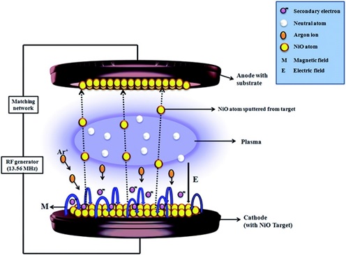
In RF sputtering, an RF power source, usually called RF signal generator replaces the conventional DC power supply, connected to the cathode in the vacuum chamber, so the electric polarity of the cathode changes alternatively. Thus, the electrons reach the target when it possesses the positive pole in the half-cycle and neutralize the positive ions collected on the target surface; while in the other half-cycle, target atoms sputtered by positive ions bombarding the target are deposited on the substrate and form a layer (Figure 1 and 2).
What is RF Sputtering?
To electrically discharge the target during sputtering a frequency of 1MHz or higher is needed. Application of an alternative current to an insulating target in this frequency range is equivalent to current flow through dielectric media of capacitors in series.
Since the frequency normally used in this method is in the range of 5-30 MHz, it is commonly known as Radio Frequency Sputtering (RF).
RF Sputtering Principles
In RF sputtering method, cathode and anode are serried with a blocking capacitor (C) (Figure 3). This capacitor is part of an impedance matching network for optimizing power transfer from RF source to the plasma. All Vac Coat RF power supplies are provided with an RF matching network to precisely tune the RF power, manually or automatically. RF voltage is an alternative voltage in the form of equation (1):
VRF(t) = VRF Sin(wt) Equation (1)
If VRF is set about 500 (V) (Figure 4-a), without blocking capacitor, the target current will be in the form of figure 4-b. Since the plasma potential is close to ground, the current density will change between Jion and –qz with changing the sign of VRF. So net current is not zero. When using blocking C and applying a self-bias DC voltage, the cathode voltage is given by Equation (2) (Figure 4-c):
Vcath(t) = VRF(t) – VDC Equation (2)
The target potential is lower than the plasma mostly. In order to reach zero net current in RF cycle, the electrode potential must be negative in most of the cycle. When the cathode potential is positive, electrons bombard the target and it is negatively charged. Since electrons have higher mobility compared to argon ions and are faster, electron bombarding time should decrease.
So duration of negatively charged target bombarding with argon ions is increased to neutralize the collected charge on the target surface (Figure 4-d). So the area under the curve of electrode current, that shows average current, is set equal to zero.
Why Frequency of 13.56 MHz is Used?
In order to prevent the interference between the frequencies used in telecommunication services, the standard radio frequency recommended by the ITU Radio Regulations (2012) for operating industrial (I), scientific (S), and medical (M) instruments, which is called ISM, is centered at 13.56 MHz with a bandwidth of 14 kHz.
Also this frequency is low enough to provide sufficient time for the momentum transfer of argon ions to the target. At higher frequencies, Ar ions are practically immobilized and electrons play effective role in the sputtering process (more like e-beam evaporation method).
A Common Problem
As mentioned earlier, insulating (Non-conductive) target materials can be deposited through RF sputtering technique. Since these materials are poor thermal and electrical conductors, they should be back-plated with a thin conductive sheet so as to prevent thermal shock and charge accumulation on the target.
The dielectric (Non-conductive) target surface should completely cover the conductive part (Backing plate) beneath, otherwise, the backing-plate is exposed to the electric field and the capacitance will be short-circuited. This is the major problem when the dielectric surface does not cover the metal backing plate in the case of plasma treatment, cleaning or coating, of dielectric surfaces.
RF Sputtering Advantages Over DC Sputtering
- The plasma formation is not limited to the cathode or target surface and can extend in the vacuum chamber
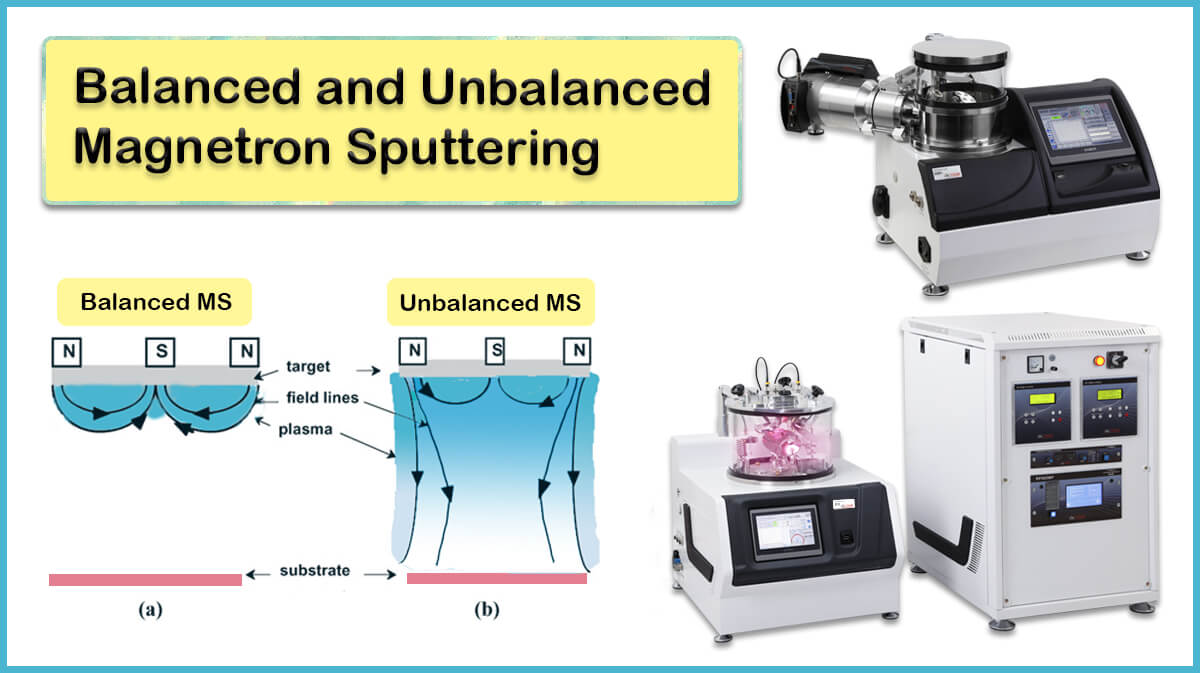
- Higher plasma currents in lower working pressure: Plasma can be maintained in less working gas pressure (1-15 mTorr), which results in less collision between sputtered atoms and chamber molecules and larger mean free path for target atoms. Also, the magnetic field of the magnetron creates a boundary tunnel which traps the electrons near target surface and increases sputtering yield in lower pressures
- By eliminating charge build up on the cathode surface, plasma arcing and layer quality control issues will be eradicated, so more uniform layer deposition is possible
- In RF sputtering larger surface of the target is involved in the sputtering process, resulting in decreasing the so called ‘Race Track Erosion’ on its surface, so the lifetime of the target is enhanced
Disadvantages of RF Sputtering (DC vs RF Sputtering)
- Compared to DC Sputtering, higher voltages should be applied in order to increase the sputtering rate, leading to more heating effect on the substrate
- This method is more complicated and expensive compared to traditional DC sputtering
- RF current is transported on the skin or surface of the conductors and not through them, so special connectors and cables is needed for RF sputtering
- With decrease in secondary electrons over cathode, deposition rate is lower than DC method and higher power level is needed to increase deposition rate
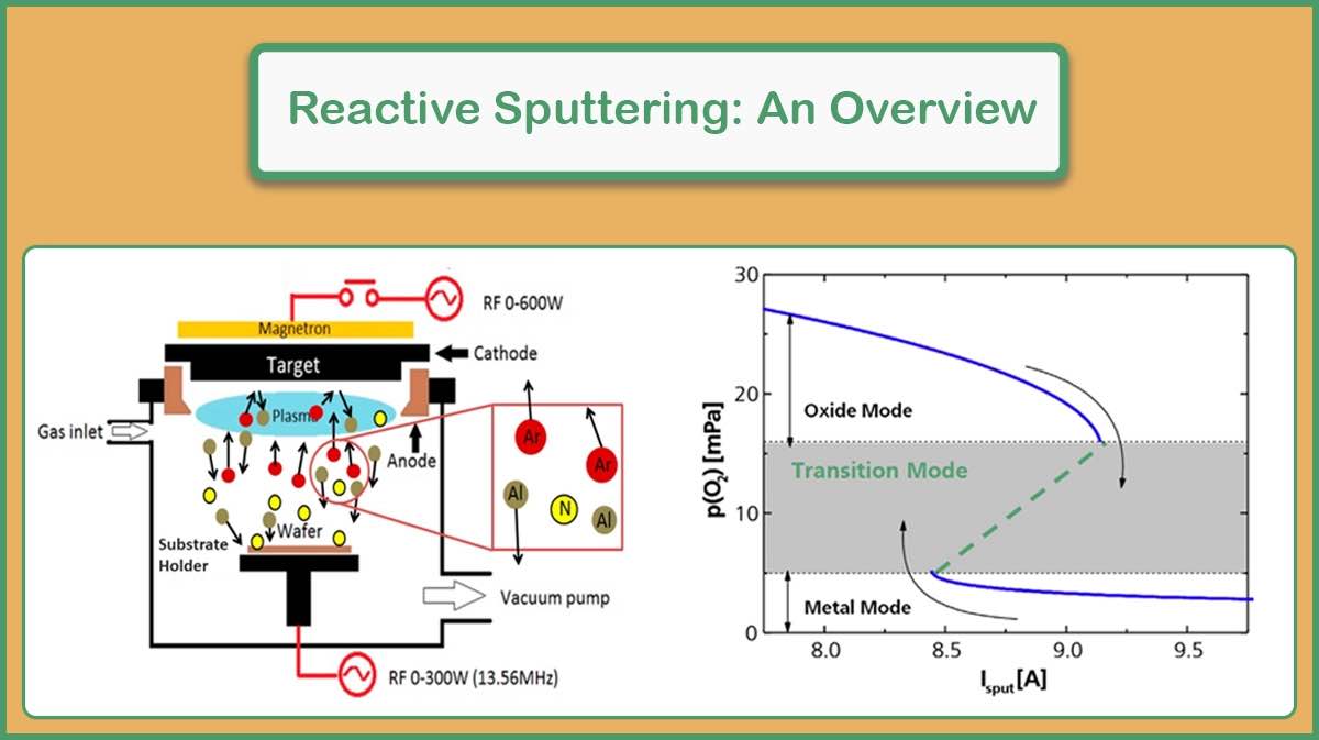
- As a consequence of lower sputtering yields of electrically insulating targets, resulting in lower deposition rates, RF sources with higher powers should be employed, in contrast to DC sputtering
RF Sputtering Systems
Vac Coat RF Sputtering Systems
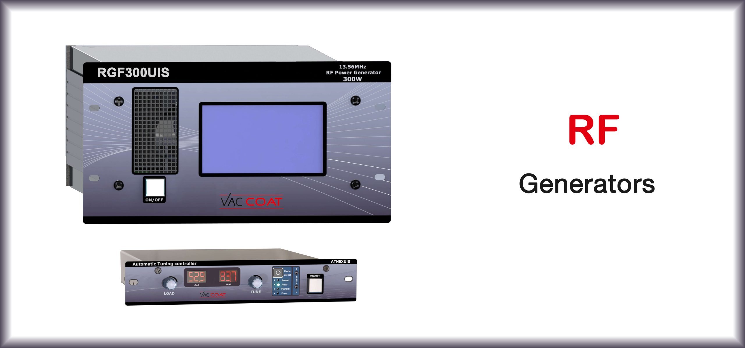
Vac Coat Ltd. offers variety of RF sputtering systems using RF generators with different powers (0.2-5 kW) supplied with precise RF matching network. The single-target sputter coater (DST1-300) and triple-target sputter coater (DST3) with thermal evaporator (DST3-T) are equipped with 600 W DC power supply and 300 W RF power supply (Optional) with auto matching box (You can read more about our sputter coaters here).
Also, plasma cleaning option is provided in these models to clean substrate surface through plasma treatment. These high vacuum sputtering systems are able to deposit wide ranges of materials, including metals, metal-oxides, semiconductors and ceramics on different surfaces for thin film applications such as micro/nano-electronics and FESEM sample preparation. You can read more about FESEM and difference between SEM and FESEM, and our SEM coaters here.
The Other Sputter Coaters
References
- https://www.sputtertargets.net/sputter-coating-technologies-radio-frequency-rf-sputtering.html
- https://www.sciencedirect.com/topics/materials-science/radio-frequency-sputtering
- “The Low Pressure Plasma Processing Environment” Donald M. Mattox, in Handbook of Physical Vapor Deposition (PVD) Processing (Second Edition), 2010
- https://baalkikhaal.github.io
- http://www.semicore.com/news/92-what-is-rf-sputtering
- “Improved electrochromic performance of a radio frequency magnetron sputtered NiO thin film with high optical switching speed” RSC Adv., 2016, 6, 79668-79680, https://doi.org/10.1039/C5RA27099E
- https://www.rfwireless-world.com/Terminology/RF-sputtering-vs-DC-sputtering.html
- https://www.tn.ifn.cnr.it/facilities/rf-sputtering-facility/rf-sputtering-principles
- Park, Sang Eun, et al. “Properties of gallium-doped zinc-oxide films deposited by RF or DC magnetron sputtering with various GZO targets.” Journal of the Korean Physical Society 54.3 (2009): 1283-1287.














Hi
I have a question. Is it possible to deposit PTFE (Teflon) by RF sputtering?
and What are normal deposition parameters?
Thanks
Yes, PTFE (Teflon) can be sputter deposited by our RF magnetron sputtering systems. Parameters may differ from device to device, reaching low or high vacuum for the base pressure, and the power is normally set under 200 W to avoid melting effects of Teflon targets.
Hi there
RF power needed to get plasma in case of copper bonded targets as compared to the unbonded sputtering targets?
RF power used to sputter the bonded or unbonded target should not be directly affected by how the target is held inside the vacuum chamber, and there should be no difference in the resulting plasma. The backing plate in bonded targets is required for efficient cooling of the target during sputtering; for uniform and controlled sputtering as well as enhancing life of the target. Inefficient cooling can lead to cracking of the target material at higher powers due to the heat load associated with sputtering process. Cu is preferred as backing plate because of its high thermal conductivity, and will efficiently remove the heat generated during the sputtering process.
How is the hydrophobicity and adhesion of PTFE (Teflon) deposited on glass by sputtering?
A hydrophobic thin film of PTFE can be deposited on the glass substrate with good adhesion by RF sputtering, considering optimization of coating parameters such as:
Besides, plasma etching of the glass substrate can enhance contact angle (increased hydrophobicity) and adhesion.
Good evening
How can we deposit Si3N4 thin film?
Hello. Si3N4 thin films can be deposited using an RF water-cooled cathode with an RF power source, utilizing power in the range of 100-200 W.
There are two methods for Si3N4 deposition:
1- By using a Si target and performing reactive RF sputtering with control over the ratio of N2/Ar+N2 gas flow.
2- By using Si3N4 target (with Indium or Elastomer bonding) with Ar/N2 gas flow to preserve the stoichiometry on the substrate.
The substrate bias voltage and temperature might be needed to be adjusted in order to obtain the required features, depending on the application.
Hello
I’m currently working on depositing NiO using reactive DC 200Watt sputtering with a NiV target. I introduce approximately 35% oxygen as a ratio. However, I’m encountering issues with reproducibility and target oxidation.
The problem I’ve noticed is that after opening the chamber, the NiV target has turned yellow, indicating NiO formation and full oxidation. I typically clean the target for 2 minutes under Argon before each deposition.
My questions are:
Should I consider extending the target cleaning duration to address the oxidation issue?
How can RF sputtering potentially help me resolve this problem and achieve more consistent NiO deposition?
Your insights and suggestions would be greatly appreciated
Thanks,
Hi.The target oxidation may be due to the high power applied to the target in the presence of oxygen containing environment. RF sputtering can lower the required deposition power and target heating, helpful for low-conductivity materials sputtering deposition. You can refer to the blog article https://vaccoat.com/blog/what-is-rf-sputtering/.
How much RF power can be applied to semiconduting targets?
RF sputtered semiconduting target should be bonded with a thin metal plate for better thermal conduction which prevents damages to the target. Hence, the sputtering power should not exceed a value of around 20 Watts/Square Inch (corresponding to 250 Watts for a 2-inch cathode), depending on the material due to the possible bonding failure. Suggested maximum power densities are based on using an optimal thermal transfer from target to the sputter cathode cooling well, otherwise it is required to reduce the suggested maximum power density and/or apply thermal transfer paste.
Reproducibility and target oxidation issue with DC sputtering 200W with NiV target with 35% O2, and NiO formation. Extend target cleaning duration before deposition? RF will help to gain more consistent NiO deposition?
The target oxidation may be due to the high power applied to the target in the presence of oxygen containing environment. RF sputtering can lower the required deposition power and target heating, helpful for low-conductivity materials sputtering deposition. You can refer to the blog article https://vaccoat.com/blog/what-is-rf-sputtering/.
I am currently working on magnetron dc sputtering to deposit carbon. It is a 9ft coating system and it shows more arcs and non uniform film . Can you please suggest the possible reasons for these problems and solutions
The deposited films coated by sputtering of carbon target usually contain high hydrogen proportions. This fact, as well as low film uniformity in this method make carbon sputtering unfavorable for SEM sample preparation. That is the reason Vac Coat company uses carbon evaporation technique in its carbon coater